Summary
The rapid development of renewable energy applications will trigger the fourth industrial revolution. Photovoltaic power generation is a key part of the entire renewable energy solution. In all solar inverters, micro solar inverters are a vital component.
This article will show you how to use a TMS320F2802 to design a low-cost, high-performance miniature solar inverter. In addition, the article will discuss how to use a cross-type active clamp flyback and SCR full bridge to achieve a 220W output miniature solar inverter, and introduce the complete system firmware architecture and control method. Finally, the article will show you laboratory waveforms.
1 Overview
1.1 Introduction of Solar Inverter
Materials, energy and information are the three major elements of human survival and development. Every new discovery of energy use will greatly change and promote the development of modern civilization:
· The invention of the steam engine brought us into the machine age.
· The invention of electricity brought us into the electrical age.
· The invention of semiconductor transistors has brought us into the information age.
The current development and utilization of renewable energy will trigger the fourth industrial revolution; in all renewable energy utilization methods, photovoltaic power generation is a key component of the development of the entire renewable energy. According to the prediction of the World Energy Organization, as traditional energy sources (such as coal, oil, etc.) are gradually depleted, renewable energy will become the main energy source for mankind. Figure 1 shows the development trend of world energy.

Figure 1 World energy development trends
Governments of all countries have paid great attention to the development of renewable energy. In 2007, the Chinese government said that "renewable energy can meet the needs of the country's long-term development plan." In 2008, the Chinese government released the 11th five-year development plan for renewable energy. According to the requirements of the plan, China's installed photovoltaic power generation capacity in 2010 needs to reach 250 billion watts; it is estimated that by 2020, China's installed photovoltaic power generation capacity will reach 500 billion watts, of which grid-connected photovoltaic power generation accounts for 75%.
The main advantages of solar photovoltaic power generation include:
· Solar energy is abundant and endless.
· The materials for producing PV panels are widely distributed and have abundant reserves.
· Simple system structure and high conversion efficiency.
· No pollution, and can be recycled.
· The photovoltaic cell has a long life and low maintenance cost.
Disadvantages of solar photovoltaic power generation include:
· Low power density and large occupied area.
· Power generation is limited by natural conditions, and power cannot be generated without the sun.
· High unit production cost.
1.2 Classification of photovoltaic power generation systems
According to the application environment, photovoltaic power generation systems can be divided into non-grid-connected solar inverter systems and grid-connected solar inverter systems.
Non-grid-connected solar inverter systems are mainly used for photovoltaic power generation systems that are independently constructed, and are suitable for communication, testing, and applications of homes, rural areas, islands, remote areas, urban lighting, and power supply systems. Figure 2 is a system structure diagram, which describes the main components of the solar panel assembly, solar inverter unit, energy storage unit, electrical load and so on.
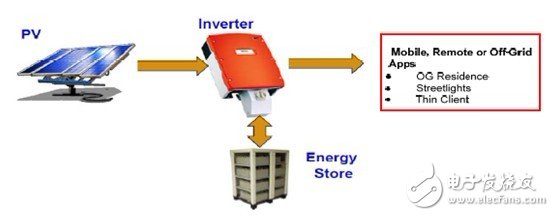
Figure 2 Non-network-connected solar inverter system
The grid-connected solar inverter system is mainly used to connect with the traditional power grid. The solar inverter connects the electrical energy from the PV panel to the traditional grid. Its main components are solar panels, solar inverters, intelligent two-way fuel gauges, household electrical loads and Traditional grid, etc. (see Figure 3)
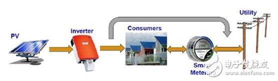
Figure 3 Network-connected solar inverter system
1.3 PV panel electrical characteristics
Solar inverter power output changes are almost directly related to sunlight, but the rate of current reduction is much faster than the decline in light level. Under very low light levels, PV panels generally produce a voltage of 16V, but the current is very small.
In addition, as the PV panel temperature increases, the voltage output decreases, and vice versa. The output curve changes with lighting conditions, temperature, etc., as shown in Figure 4.
The solar inverter must work under MPP to obtain the maximum power from the PV panel. This is achieved through the maximum power point control loop (Maximum Power Point Tracker, MPPT).
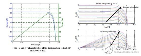
Figure 4 PV panel electrical characteristics
1.4 Topology change of solar inverter
With the change of illuminance, the output voltage of the PV panel ranges from 20 to 45 volts. Therefore, if a higher output voltage is required for grid-connected applications, the PV panel is usually considered and connected in series to obtain a high input voltage, and an inverter is used to To achieve electrical energy conversion. This topology is called "central inverter", as shown in Figure 5 (a); its main features are:
· 10 to 250kw, 3 phases, several parallel strings
· High converter efficiency, low cost and low reliability
· Non-optimal MPPT
· Usually used in power plants
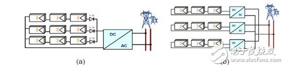
Figure 5 Central and string topology
Another application is to connect PV panels in series at all string branches to achieve energy conversion. An MPPT module is used to obtain the maximum power of the PV panel. This topology is called "string inverter", as shown in Figure 5 (b); its main features are:
· 1 to 10kw, typical residential applications.
· Each string branch has its own inverter for better MPPT.
· Each string can have a different direction.
· Three-phase inverter for output power over 5km.
Although this string inverter can obtain more power collection efficiency, when a series PV panel is blocked by shadows, the power collection of the string branch also decreases, as shown in Figure 6 (a). If an MPPT module is placed to collect the electrical energy of all PV panels, this problem can be solved. This topology is called "micro inverter", as shown in Figure 7.

Figure 6 The effect of shadow on power collection 
Figure 7 Micro-inverter topology
Obviously, as far as micro-inverters are concerned, the “distributed MPPT†architecture increases the cost per PV panel; however, the efficiency can be increased by 5% to 25% by recovering the following efficiency losses:
· PV panel mismatch loss (3% to 5%)
· Partial shadow loss (5% to 25%)
· Simple system design, looser fault tolerance (0% to 15%)
· Sub-optimal MPPT loss (3% to 10%)
· In addition, increase safety and construction area (roof) utilization
Therefore, if we choose a micro-inverter topology, the efficiency of the converter will be sacrificed, but the energy collection will become more efficient.
2 Hardware design
2.1 System structure diagram
In our solar inverter solution, we choose the topology of cross flyback plus SCR full bridge for industrial frequency inverter. All control is only one MCU (2802x), and there is also an RS485 or PLC interface for communication. Figure 8 shows the structure of this micro solar inverter. For specific specifications, please refer to Annex A.
This topology has the following characteristics:
· Simple system structure
· High efficiency, low cost
· Complete isolation, high reliability
· Reactive power compensation cannot be achieved

Figure 8 Micro solar inverter system structure diagram
2.2 Auxiliary power design
In micro solar inverters, we need auxiliary power supplies that can output multiple voltages to A / D sampling circuits, drive circuits, MCU controllers, etc. On the other hand, this auxiliary power supply must be completely isolated from the primary side to the secondary side.
Therefore, we choose the LM34927 chip; this chip has the following characteristics:
· Wide input range of 9 to 100V
· Low cost, integrated 100V, high and low side switch
· The constant on-time (COT) control scheme does not require loop compensation and has excellent transient response.
· Full protection function, including adjustable UVLO.
Figure 9 shows a typical application schematic of the LM34927. From this schematic, we know that the primary side of the LM34927 is a buck circuit, while the secondary side is a flyback topology for isolation.
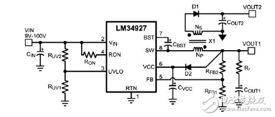
Figure 9 LM34927 typical application schematic
2.3 Active clamp flyback designed as an isolated front-end converter
2.3.1 Overview of Active Clamp Flyback Converter
Figure 10 shows the combination of active clamp circuits in the basic flyback topology. In the figure, the flyback transformer is replaced by an equivalent circuit model, which shows magnetization and leakage inductance (Lr represents the total transformer leakage inductance reflected on the primary side except the external inductance).
Switches Q1 and Q2 appear together with their associated body diodes. Cr represents the parallel capacitance of the parasitic capacitance of the two switches. This device capacitance resonating with Lr realizes the zero voltage switching (ZVS) of Q1.
With the active clamp circuit, the transistor off voltage spikes are controlled, the transformer leakage is recovered, and the ZVS of both the main switch (Q1) and the auxiliary switch (Q2) becomes possible.
The cost of these advantages is the need for more power stage components and higher control circuit complexity (two switches to one switch).
To describe the operation of this circuit, we assume:
· Ideal switch assembly
· The magnetizing current is always non-zero and positive.
· Lr (including transformer leakage inductance) is less than transformer magnetizing inductance Lm (usually 5% to 10% of Lm)
· Store enough energy in Lr to completely discharge Cr and turn on the body diode of Q1.

Figure 10 Simplified schematic diagram of an active clamp flyback converter
2.3.2 Zero-voltage switch considerations for active clamp flyback design
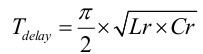
In order to achieve the ZVS of Q1, Q2 must be turned on during the drop of the resonant inductor current. Otherwise, the resonant inductor current reverses (becomes positive again), it recharges Cr, and loses ZVS (or at least partially). Therefore, the delay time between turning off Q2 and turning on Q1 is critical to ZVS operation. The optimal delay value is a quarter of the resonance time formed by Lr and Cr:
Therefore, it is best to set the dead time between Q1 off and Q2 on, less than Tdelay, to achieve a partial ZVS state.
Even if the stored energy in Lr is not enough to completely discharge the switched capacitor Cr, thereby minimizing the potential voltage stress of Q1 and Q2 (and obtaining higher converter efficiency), we must carefully design the resonant inductor Lr, resonant capacitor Cr, and clamp The parameter of the bit capacitance Cc.
2.3.2.1 Design of resonant inductor Lr
After determining the Lm value, the resonant inductance can be designed. As mentioned earlier, we assume that its value is a small part of Lm (usually 5% to 10% of Lm).
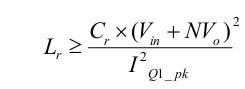
Given the converter operating point and Cr value, to achieve ZVS, the size of Lr must be sufficient to fully discharge the switched capacitor.
Lr design is difficult because the resonant capacitor voltage (Vcr) is a function of the Lr value, as shown in the following equation:
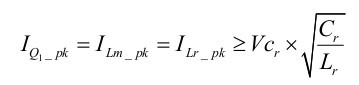
However, in actual design, the resonant inductor voltage is relatively small (relative to Vin + NVo), and the approximate minimum value of Lr necessary to achieve the ZVS state can be solved:
In such applications that require high output voltages, the special output rectifier soft-switching characteristics are more ideal than implementing the main switch ZVS.
2.3.2.2 Cc design of clamping capacitor
According to the Lr design, select the value of the clamping capacitor. The resonant frequency formed by the clamping capacitor and the resonant inductor is low enough so that when the switch is closed, the power switch will not have excessive resonant ringing. However, using an excessively large clamping capacitance value will not bring about an improvement in clamping performance, and the cost will be a larger (and more expensive) capacitor. A better compromise is to choose a capacitor value such that half of the resonance time formed by the clamping capacitor and the resonant inductor exceeds the maximum off time of Q1. therefore:

Among them, DHL represents the maximum input voltage operation, and fs is the working switching frequency of Q1 and Q2.
The rated voltage of the capacitor must exceed NVo, and the excess voltage is Lr:

The resonance time of the clamp capacitor and resonant inductor can be calculated by the following equation:

2.3.3 Open-loop simulation of active clamp flyback
Figure 11 shows the open-loop simulation model of this active clamp flyback. The following values ​​are used for this simulation: input voltage Vin = 36V, main MOSFET switching frequency fs = 65kHz, resonant inductance Lr = 0.5µH, resonant capacitor Cr = 1nF, clamping capacitor Cc = 10µF, maximum duty factor D of main switching MOSFET = 0.6, and the load Rload = 100 Ω.
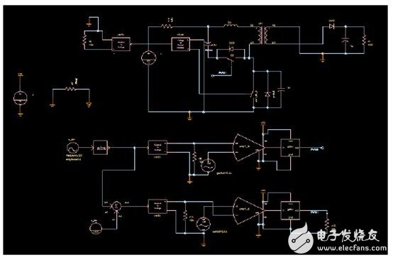
Figure 11 Open-loop simulation model of active clamp flyback 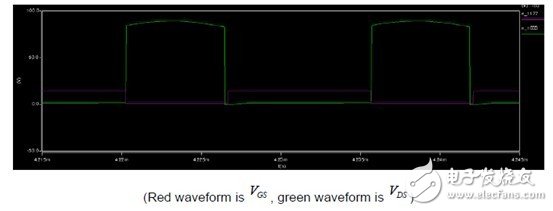
(The red waveform is VGS and the green waveform is VDS)
Figure 12 Q1 VDS and VGS simulation waveforms
Figure 12 shows that the gate drive voltage rises after the drain-to-source voltage drops to zero, so Q1's ZVS implementation is confirmed. In addition, the voltage spike of VDS is clamped to Vin + NVout, which means that the active clamping is implemented on the primary side.

Figure 13 Simulation output voltage waveform
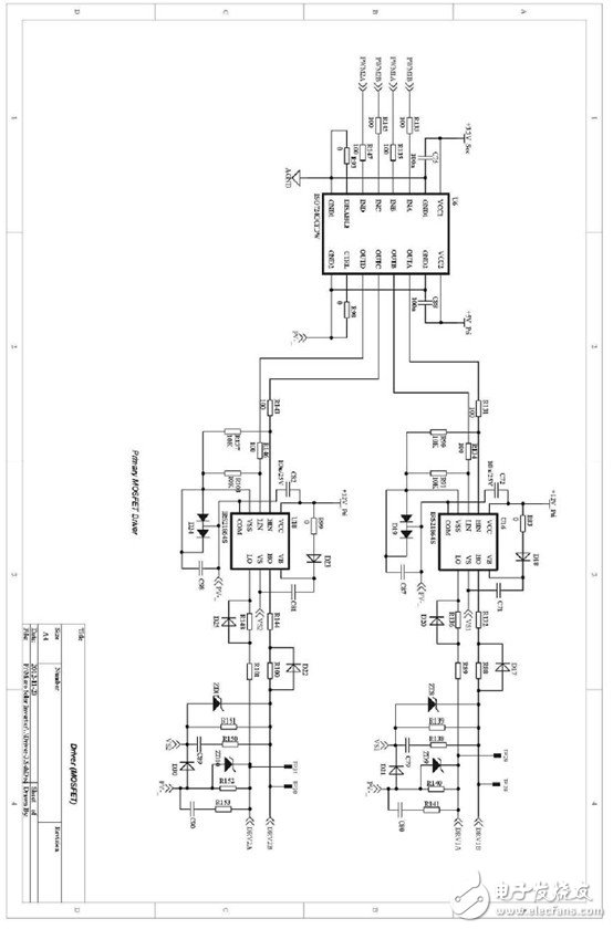
2.4 Design of isolated MOSFET bridge drive circuit
In order to achieve complete isolation from primary side to secondary side, in addition to auxiliary power isolation, A / D sampling and drive circuit isolation are also required.
Since the MCU is placed in the secondary side and the main switch MOSFET is on the primary side, we must transmit the secondary side control signal to the primary side to control the MOSFET.
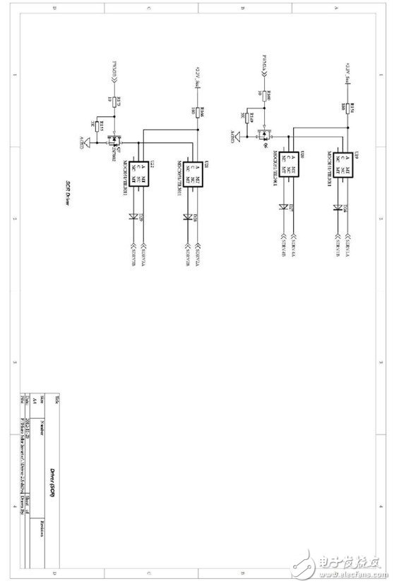
In order to transfer the control signal from the secondary side to the primary side, a high-speed digital isolator plus a high-end driver chip can be selected. Figure 14 shows the schematic of this isolated MOSFET high and low side driver.
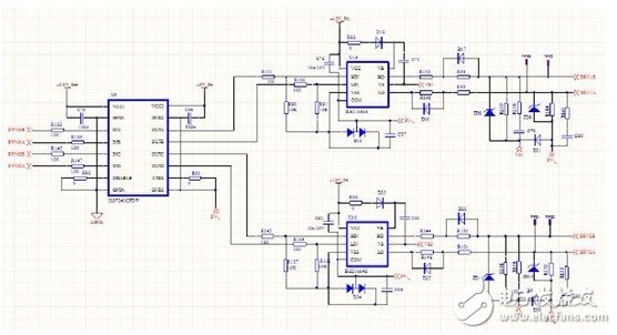
Figure 14 Schematic diagram of isolated high and low end drivers
In this application, the isolated MOSFET has many characteristics, including:
· Simple structure, easy to realize
· + 600V full working range
· 4kV ESD protection
· Boot job
In addition, please pay attention to the initial state of the high-speed digital isolator; otherwise, it will damage the main switching MOSFET.
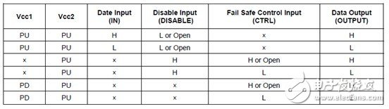
Table 1 High-speed digital isolator function table
(PU = power on; PD = power off; X = do n’t care; H = high level; L = low level)
3. Firmware design
3.1 Firmware specification
3.1.1 Functional specifications
The system firmware includes the following functions:
1. On / off. The user can turn the system on or off by pressing the on / off button. Software settings must enable this feature.
2. Automatic on / off. If it needs to be turned on, the system will automatically turn on. When the state is not suitable for power transmission to the grid, the system maintains the standby mode and monitors the state changes. If the system has been turned on, the system automatically turns off when the state is not suitable for power supply.
3. The software starts and starts. When the system must be turned on, it starts from the zero current supply state, and the PWM is turned on at the zero crossing point, thereby reducing the inrush current brought to the grid.
4. LED control. The system has a status LED indication. When the system is in standby mode, the corresponding LED flashes once every 1.2 seconds. When the system is turned on, the LED flashes every 2.4 seconds. When a fault occurs, the LED lights continuously.
5. User control keys. The inverter has a user key. This user key can turn on or off the inverter, and can also clear the fault. When the system is in standby mode, if the key is pressed for more than 1 second, it will turn on if the conditions are met. If the system has been turned on, when the key is pressed for more than 1 second, the system is turned off. When a fault occurs and the system is in fault mode, press this user key for more than 1 second to clear the fault and enter standby mode again.
3.1.2 Measurement
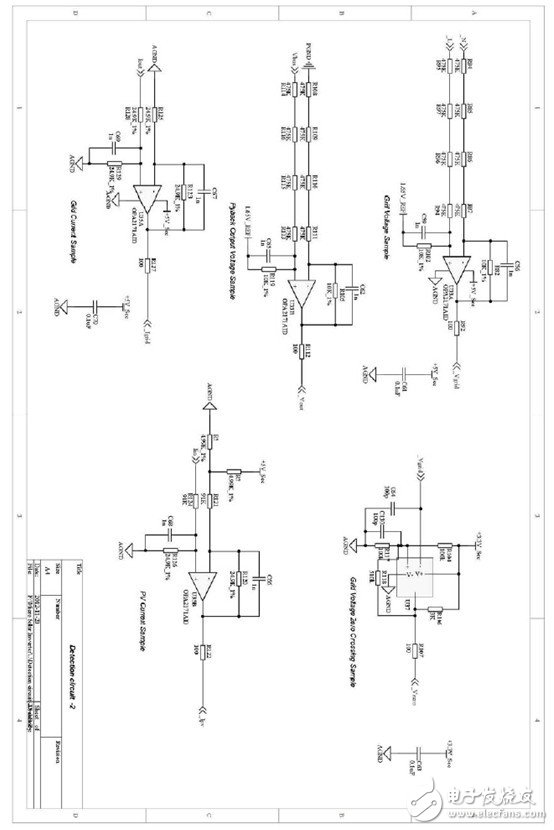
In order to control and monitor the system status, the following measurement results need to be calculated:
· Grid voltage RMS
· Grid frequency
· Inverter output effective power
· Input power
· Input PV voltage
· Temperature
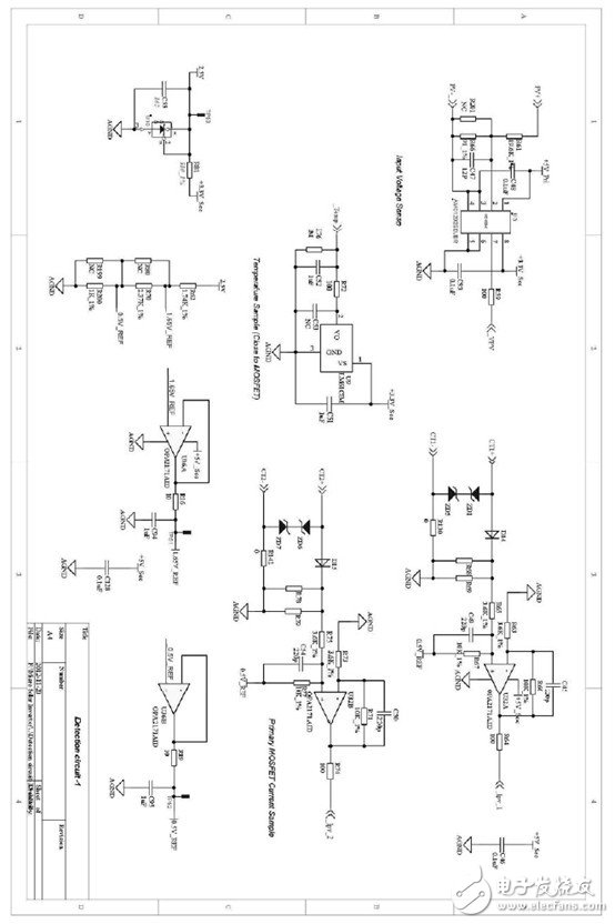
3.1.3 Protection
The system has some basic protection functions.
1. Primary side inrush current protection. When short-circuit or main inductance causes an inrush current, the PWM first enters CBC mode; however, when CBC is more than three times, the system shuts down and enters fault mode.
2. Secondary side overvoltage protection. When the SCR is not normally turned on, the secondary side ultra-high pressure appears. The system shuts down and enters failure mode.
3. Output overcurrent protection. When the output current exceeds the threshold, output overcurrent occurs. The system shuts down and enters failure mode.
4. Grid voltage / frequency too high / low protection. If the system has been turned on, when the grid voltage / frequency exceeds the normal range, the system will shut down within five grid cycles.
5. Anti-island suppression protection. If the island condition is reached, the system shuts down within 4 seconds. If it returns to the normal state, the system restarts within 1 second.
6. Over-temperature protection
3.1.4 Network converter controller
In order to transmit power to the grid, the following controller algorithms must be implemented in the system:
1. Phase-locked loop (PLL) controller. The PLL controller is used to synchronize with the grid voltage, and it can provide a reference phase to the current controller.
2. Network current controller. The current controller ensures that the output current is a sine wave and follows the current reference to balance the input power and output power.
3. Maximum power point tracking (MPPT). MPPT is used to make the solar panel enter the maximum power output state.
3.2 Firmware structure
3.2.1 Background and tasks
The entire firmware system is a forward-facing background system. Figure 15 shows the background structure.
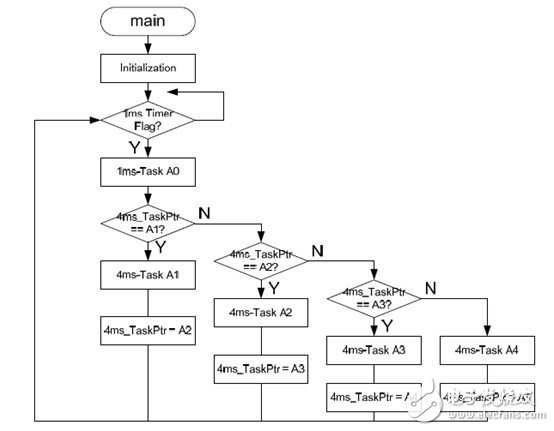
Figure 15 background structure
In this system, there is a 1ms task and four 4ms tasks.
1. 1ms task A0. 1ms regular task. In this task, LED control is executed. In addition to this, the PLL controller is also located in this task.
2. 4ms task A1. A1 4ms periodic tasks. State machine processor.
3. 4ms task A2. A2 4ms periodic tasks. All measurements are calculated in this task.
4. 4ms task A3. A3 4ms periodic tasks. User key detection is here, at the same time it detects that it exceeds or does not reach the operating state range, and issues a fault command.
5. 4ms task A4. A4 4ms periodic task. MPPT controller and debugging support.
3.2.2 System state machine

Figure 16 State Machine
Figure 16 shows the state machine processed in task A1. Different states represent different operating modes.
There are 4 status modes in this system:
· Power on
· Standby
· Open
· Fault
Power-on mode is a transitional mode of system power-on. In this mode, the system performs some initialization, after which, the system automatically enters standby mode.
Standby mode is a mode in which the system waits for an open command. All PWM and SCR control signals are turned off. In this mode, all measurements are valid. The system detects the external status and checks whether the system can be turned on.
After the system successfully starts from the standby mode, the system enters the on mode. In this mode, all PWM and SCR control signals are turned on. The system begins to transmit power to the grid.
If a fault occurs, the system enters the fault mode and all PWM and SCR control signals are turned off. If the fault is cleared, the system automatically returns to standby mode.
3.2.3 Interrupt service routine
The interrupt service routine (ISR) of this system has the following functions:
· Read ADC results and some measurement calculations.
· Network current controller
· SCR on / off control
· Emergency protection. Primary side inrush current, secondary side overvoltage and output current protection.
· Debugging support. Record the debug data to the buffer.
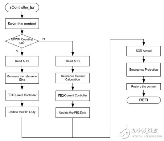
Figure 17 ISR flow chart
3.3 Network converter controller
Figure 18 shows the entire network converter structure.
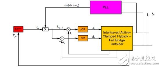
Figure 18 Controller structure
3.3.1 PLL controller
Figure 19 shows the PLL controller system
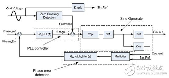
Figure 19 PLL control system diagram
The PLL system consists of the following parts:
· Phase error detection. Detect the phase error between the reference and the sine wave output. This detection function is implemented in 1ms task A0.
· PLL controller. Closed loop controller, the controller executes in 1ms task A0.
· Sine wave generator. Generate a sine wave based on frequency and sampling time; accomplish this in the ISR.
3.3.2 Current controller
In order to design the current loop, the object model must first be built. A small signal model can be used here.
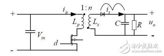
Figure 20 Flyback circuit
It is assumed that the flyback circuit is shown in FIG. 6; in addition, it is assumed to operate in continuous mode.

Figure 21 Flyback continuous mode current
If the MOS on the primary side is turned on, the primary current increases, Lp charges, and energy is stored inside. Therefore, the following equation can be obtained:

If Q1 is turned off, the energy is immediately transferred to the secondary side, and ip quickly drops to zero. On the secondary side, the diode is turned on, the secondary inductance is connected to the load, and C is charged. Equation (2) can be obtained.
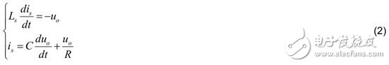
The main inductance Lp and the secondary inductance Ls have the following relationship:

Combine equation (3) with equation (2) to get:

Using this average state space method, if the duty factor is d, the following equation can be obtained:
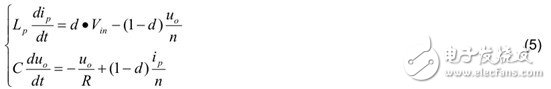
The other party's program (5) is slightly modified to obtain:
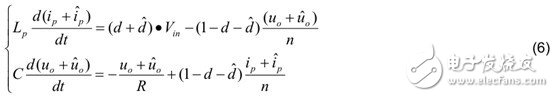
Removal of high-order infinitesimal elements yields:

therefore,  with
with  The relationship is:
The steady state of D is:

The controller loop is:
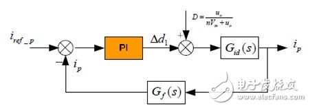
Figure 22 Current controller loop
When using a PI controller, the controller calculates a frequency of 22kHz. The open loop bandwidth must be set to 1 to 2kHz.
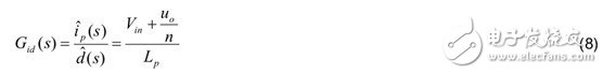
Figure 8 shows that the closed-loop feedback must be the primary current ip, but in a real system, it is the midpoint current when Q1 is turned on. If the converter is operating in continuous mode, the relationship between primary feedback and secondary average current is:

In order to obtain a sine wave output current, the secondary average current must be a sine wave; therefore, the feedback circuit must be changed to the following model:
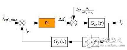
Figure 23 Modified current loop
4 Laboratory test waveform

(CH3 closed-loop output voltage, CH4 closed-loop output current)
Figure 24 Closed-loop output current and voltage 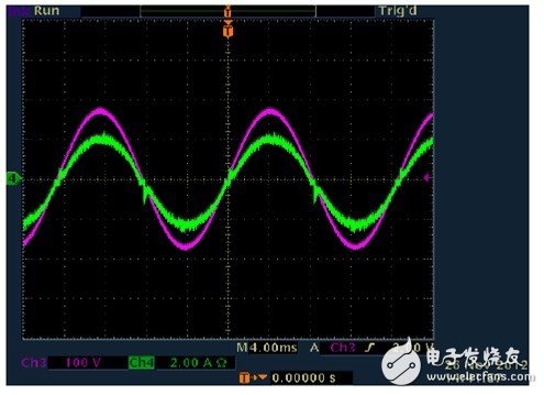
(CH3 network voltage, CH4 network current)
Figure 25 Network current and network voltage 
(CH2 network voltage, CH4 network current)
Figure 26 Voltage and current waveforms when the system is turned on 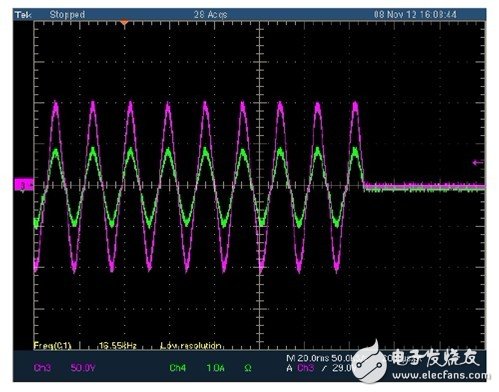
(CH2 network voltage, CH4 network current)
Figure 27 Voltage and current waveforms when the system is off 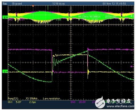
(CH1 VGS of main switching MOSFET, CH3 VDS of main switching MOSFET, CH4 resonance current of Lr)
Figure 28 ZVS waveform and Lr resonance current of the main switching MOSFET 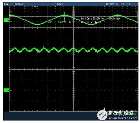
(CH4 grid current ripple)
Figure 29 Incoming current ripple
5 Other
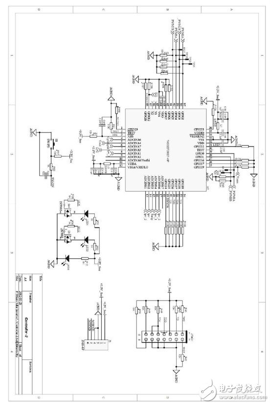
Principle diagram, please refer to "Annex B"
6 References
1. TMS320F2802x product manual, SPRS523G
Appendix A, Electrical Specifications 
Appendix B. Schematic diagram 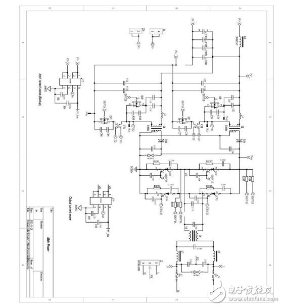


Door Mat,Front Door Mat,Door Mat Outdoor,Outdoor Door Mat
Cixi Mingsheng Rubber & Plastic Co.,Ltd. , https://www.cixidoormats.com