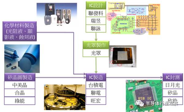
The focus of this article is on what the semiconductor industry is doing from upstream to downstream. First look at the correlation diagram:
We first understand the general direction, and then explain in detail.
The most upstream of the semiconductor industry is IC design companies and silicon wafer manufacturing companies. IC design companies design circuit diagrams based on customer needs, and silicon wafer manufacturing companies use polycrystalline silicon as raw materials to manufacture silicon wafers. The main task of the IC manufacturing company in the middle is to transplant the circuit diagram designed by the IC design company to the wafer manufactured by the silicon wafer manufacturing company. The completed wafers are then sent to the downstream IC packaging and testing factory for packaging and testing, and you're done!
Partial commentary begins!
(1) Silicon wafer manufacturing
The most upstream of the semiconductor industry is silicon wafer manufacturing. In fact, the upstream silicon wafer industry is formed by three sub-industries, followed by the initial purification of silicon → polysilicon manufacturing → silicon wafer manufacturing.
Preliminary purification of silicon:
Convert quartz sand (SiO2) into metallurgical grade silicon (silicon purity above 98%).
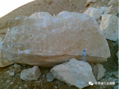
Quartz sand.
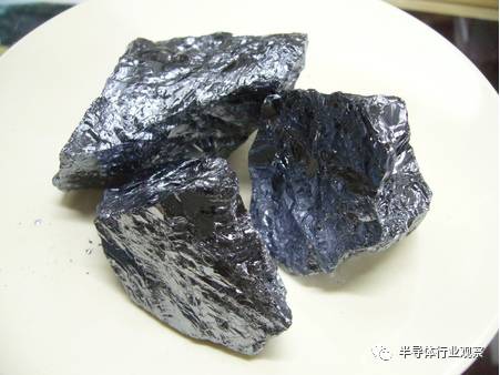
Metallurgical grade silicon.
Polysilicon manufacturing:
The metallurgical grade silicon is made into polycrystalline silicon. The polysilicon here can be divided into two types: high purity (99.999999999%, 11N) and low purity (99.99999%, 7N). High purity is used to make ICs and other precision circuit ICs, commonly known as semiconductor grade polysilicon; low purity is used to make solar cells, commonly known as solar grade polysilicon.
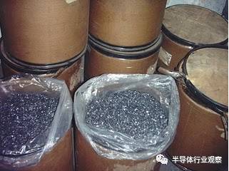
Polysilicon.
Silicon wafer manufacturing:
Polycrystalline silicon is made into silicon wafers. Silicon wafers can be divided into single crystal silicon wafers and polycrystalline silicon wafers. In general, silicon wafers used for IC manufacturing are single-crystal silicon wafers, and silicon wafers used for solar cell manufacturing are both single-crystal silicon wafers and polycrystalline silicon wafers. Generally speaking, the efficiency of monocrystalline silicon will be higher than that of crystalline silicon, of course, the cost is also higher.
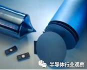
Silicon wafer
(2) IC design
As mentioned earlier, the manufacture of silicon wafers uses quartz sand and produces silicon wafers. The input of IC design is the superb brain (and liver) of the "good people", and the output is the circuit diagram, and finally the photomask is sent to the IC manufacturing company, and the merit is completed!
However, it is not easy to let people outside the science and technology department understand IC design (just like to let people who study science and technology understand complex derivative financial commodities), the author must go through many times to get materials . Here is probably a concept, please use your strong imagination!
In simple terms, IC design can be divided into several steps, in order: specification development → logic design → circuit layout → post-layout simulation → mask making.
Specification development:
The engineers of the brand factory or the white brand factory (the brand factory without a brand) contact the IC design engineer and issue the specifications of the IC they need to the IC design engineer (for example, the first foot position and the second foot position Add to be equal to the ninth pin). After discussing the specifications, the engineers started to work happily!
Logical design:
With the help of the software, the engineers have finally completed the logic design diagram, take a look:
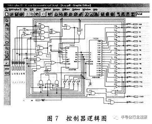
Controller logic diagram
The so-called "logic" design drawing refers to that it is composed of simple logic components, rather than the disgusting semiconductor circuit components (such as diodes, transistors, etc.) mentioned in this semiconductor type. Forget to review it. !) Constituted. What is a logic element? Such as AND Gate (as the name implies, if both inputs are 1, the output is 1, otherwise the output is 0), OR Gate (as long as one of the two inputs is 1, the output is 1) and so on. The logic components will be further introduced to you in the IC design unit.
Circuit layout:
Basically, it is to use the help of software to transform a friendly logic design into a disgusting circuit diagram. As shown:
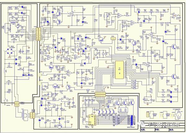
Integrated circuit diagram.
Everyone should be familiar with it! Most of them are diodes and transistors that we have found in the semiconductor category!
Post-layout simulation:
Just check the software again to see if the result is the same as the original "specification"!
Mask making:
After the circuit is completed, make the circuit into a piece of photomask and you're done! The completed photomask is sent to the IC manufacturing company. Let's see what the photomask looks like!
Photomask.
(3) IC manufacturing
The IC manufacturing process is more complicated, but in fact IC manufacturing only does one thing: transfer the circuit diagram on the photomask to the wafer. Its process is actually very similar to the traditional photo manufacturing process (of course, the precision is too bad)! If you go online and google "IC manufacturing", you will see a lot of Martian information, ensuring that you don't understand what those processes mean.
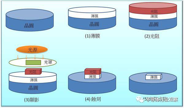
The steps of IC manufacturing are as follows: film → photoresist → development → etching → photoresist removal, and then circulate for dozens of times. Let's take a look at the schematic
IC process.
film:
Plated with metal (actually not necessarily metal)
Photoresist:
Apply a layer of photoresist (photosensitive layer) on the wafer
development:
After passing through the "mask" with strong light, it shines on the wafer. In this case, except for the part where the "circuit" should appear, does the rest of the photoresist shine on the light?
Etching:
Erosion of the film without photoresist coverage
Photoresist removal:
Remove the photoresist above, and the part of the film left is the circuit diagram! (It is assumed here that the circuit diagram is just a "long bar", but the actual situation is of course more complicated!)
It's simple! Of course, the actual process is not that simple. The actual situation is that the photomask is composed of dozens of layers, and the materials required for each layer are different. In other words, the film layer needs to use different materials. For example, SiO2.
Interesting! The above is just an introduction, there will be a more detailed introduction in the "Semiconductor Manufacturing" unit!
(4) IC packaging and testing
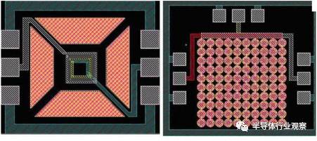
The IC completed by the IC manufacturer is roughly as follows:
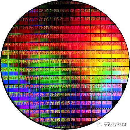
Wafer finished product.
This piece of finished wafer is sent to the IC packaging and testing factory for IC packaging and testing.
Package:
The packaging process is roughly as follows: cutting → pasting → welding → mold sealing.
Let ’s talk about the concept first, let ’s look at a CPU!
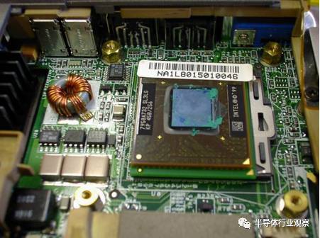
CPU.
In the center of the picture is the CPU. The CPU is a big one, but if you look closely, the metal part in the middle is the real size of the CPU bare crystal (also called the die, that is, the IC before unpacking)! The rest is the so-called PCB-PCB!
it is good! You can start talking about IC packaging!
Cutting:
The first step is to cut the wafers sent by the IC manufacturing company into rectangular ICs!
Paste:
Paste the IC to the PCB
welding:
As the name implies, solder the small pins of the IC to the PCB so that it is compatible with the large PCB (such as the motherboard)!
Mold seal:
As the name implies, it is to seal the pin mold. The hot topic recently-BT resin, is used here!
Do you feel Looking at a picture is more clear:
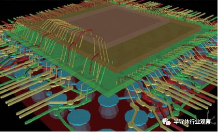
IC products.
As shown in the figure, the middle is the die, which is externally connected to the PCB.
This is almost complete! Detailed packaging and testing flow chart, we will introduce in detail in the IC packaging and testing sheet, so stay tuned!
It's not easy! Finally, the general production process of an IC is introduced!
We main Produce many style Disposable Vape,for example:puff flex, Elf Bar 5000,elf bar 5000 ultra.elf bar 1500 ,Crystal Legend Vape,Fluum Bar Vape,Elf Bar Lost Mary,RandM Tornado Vape Uk,Elfworld Disposable Vape,Elfbar 600,KK Energy Vape and so on.welcome contact .
Electronic Cigar,Health Electronic Cigarette,Mini Electronic Cigarette,Vape Electric Cigarette,Disposable Vape
Shenzhen Ousida Technology Co., Ltd , https://www.osdvape.com