(This article is contributed by Synopsys and published on the e-enthusiast platform)
Over the past decade, several technological advancements have made artificial intelligence (AI) one of the most exciting technologies. In 2012, Geoffrey Everest Hinton demonstrated his generalized back propagation neural network algorithm in the Imagenet Challenge, which revolutionized the field of computer vision. However, the machine learning theory was proposed as early as 2012, and microprocessors such as the Nvidia GTX 580 graphics processor unit made this theory possible. These processors have relatively high memory bandwidth capabilities and are good at matrix multiplication, which can shorten the AI ​​training time of the neural network model to about one week. The combination of theory and algorithm has opened up a new generation of technological advancement and brought new possibilities related to AI. This article outlines the new era of artificial intelligence design and its diverse processing, memory, and connectivity requirements.
Anatomy of Artificial Intelligence
We define neural network as deep learning, which is a subset of machine learning and artificial intelligence, as shown in Figure 1. This is an important category, and this subset of deep learning has changed the chip system architecture design.
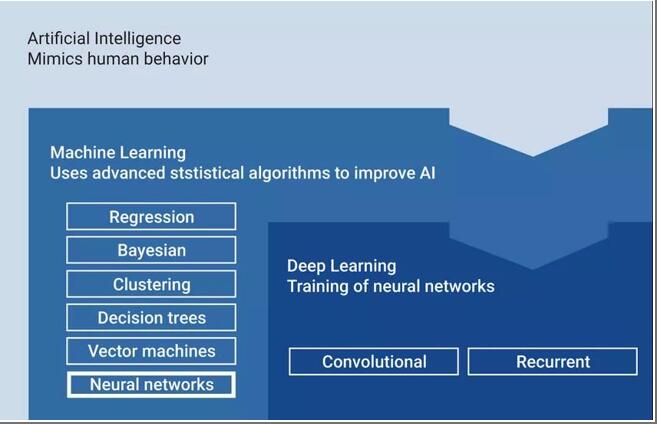
Figure 1: Artificial intelligence uses deep learning algorithms to imitate human behavior
Deep learning not only changed the chip architecture, but also spawned a new round of investment in the semiconductor market. Deep learning algorithm models are a hot spot for R&D and commercial investment, such as Convolutional Neural Networks (CNN). CNN has always been the main focus of machine vision. Models such as recurrent neural networks are used in natural language understanding because of their ability to recognize time.
Artificial intelligence applications
Deep learning neural networks are used in many different scenarios, providing powerful new tools for those who use them. For example, they can support advanced security threat analysis, predict and prevent security breaches, and help advertisers identify and streamline the sales process by predicting the shopping process of potential buyers.
But AI design is not limited to data centers. Many new features such as visual systems for object and face recognition, natural language understanding for improved human-machine interfaces, and surrounding environment perception can be used to make machines understand based on a combination of sensor inputs. Activities that are happening. These deep learning capabilities have been integrated into the chip design required for different scenarios, including smart cars, digital homes, data centers, and the Internet of Things (IoT), as shown in Figure 2.

Figure 2: AI processing capabilities have been integrated into a large number of applications
Mobile phones use neural networks to achieve the above-mentioned multiple AI functions. The mobile phone can run face recognition applications, object recognition applications, and natural language understanding applications. In addition, it uses neural networks for 5G self-organization internally, because wireless signals become denser on other media and different spectra, and the transmitted data has different priorities.
Human brain
Recently, deep learning has become feasible through advances in mathematics and semiconductor hardware. The industry has launched a number of initiatives to better replicate the human brain in the next generation of mathematical models and semiconductor architectures, which is often referred to as neuromorphic computing. The human brain can achieve incredibly high efficiency, but technology has only just begun to scratch the surface in terms of replicating the human brain. The human brain contains more than 1 PB (Petabyte=1024TB) of storage space, which is equivalent to about 540 trillion transistors, and the power is less than 12 watts. From this point of view, duplicating the brain is a long-term goal. However, the ImageNet Challenge has evolved from the first backpropagation CNN algorithm in 2012 to the more advanced AI model ResNet 152 in 2015. The market is developing rapidly, and new algorithms are emerging in endlessly.
AI design challenges
The chip architecture that integrates deep learning capabilities has promoted the advancement of a number of key technologies, so as to achieve highly integrated solutions and more general AI chips, including dedicated processing requirements, innovative memory architectures, and real-time data connections.
?? Dedicated processing needs
Chips incorporating neural network capabilities must adapt to both heterogeneous and massively parallel matrix multiplication operations. Heterogeneous components require scalar, vector DSP and neural network algorithm capabilities. For example, machine vision requires independent steps, and each step needs to perform different types of processing, as shown in Figure 3.

Figure 3: Neural network capabilities require unique processing
Preprocessing requires simpler data-level parallelism. Accurate processing of the selected region requires more complex data-level parallelism, which can be effectively processed by a dedicated CNN accelerator with good matrix multiplication capabilities. The decision-making stage can usually be handled by scalar processing. Each application is unique, but it is clear that heterogeneous processing solutions including neural network algorithm acceleration need to effectively process AI models.
Innovative memory architecture
The AI ​​model uses a lot of memory, which increases the cost of the chip. Training neural networks requires several GB or even 10 GB of data, which requires the use of the latest DDR technology to meet capacity requirements. For example, VGG-16 as an image neural network requires approximately 9 GB of memory during training; a more accurate model VGG- 512 requires 89GB of data to train. To improve the accuracy of AI models, data scientists use larger data sets. Again, this will increase the time required to train the model or increase the memory requirements of the solution. Due to the need for massively parallel matrix multiplication operations and the size of the model and the number of required coefficients, this requires external memory with high-bandwidth access capabilities and new semiconductor interface IP, such as high-bandwidth memory (HBM2) and derivative products ( HBM2e). Advanced FinFET technology supports larger chip SRAM arrays and unique configurations, with customized memory-to-processor and memory-to-memory interfaces. These technologies are under development to better replicate the human brain and eliminate memory constraints.
The AI ​​model can be compressed, which is necessary to ensure that the model runs on the constrained memory architecture in chips located at the edge of mobile phones, automobiles, and IoT applications. Compression is performed using pruning and quantization techniques and cannot reduce the accuracy of the results, which requires traditional chip architecture (with LPDDR or in some cases without external memory) to support neural networks. With the compression of these models, irregular memory access and computational intensity increase, which prolongs the execution time of the system. Therefore, system designers are developing innovative heterogeneous memory architectures.
Real-time data connection
Once the AI ​​model is trained and possibly compressed, real-time data can be executed through many different interface IP solutions. For example, vision applications are supported by CMOS image sensors and connected via MIPI camera serial interface (CSI-2) and MIPI D-PHY IP. LiDAR and radar can be supported by a variety of technologies, including PCI Express and MIPI. The microphone transmits voice data through USB, pulse density modulation (PDM) and I2S connections. Digital TV supports HDMI and DisplayPort connections to transmit video content, and these content can be improved after transmission through a neural network to achieve ultra-high image resolution, thereby generating higher-quality images with less data. Currently, most TV manufacturers are considering deploying this technology.
Hybrid AI systems are another concept that is expected to be adopted in large numbers. For example, the heart rate algorithm can identify abnormalities through the AI ​​system on the fitness belt. By sending the information to the cloud, the abnormalities can be analyzed more accurately and in-depth by the AI ​​neural network and prompted. This type of technology has been successfully applied to the balance of grid load, especially in the case of power line interruption or unexpected heavy load. In order to support fast and reliable network and cloud connections, the aggregator in the above example requires an Ethernet connection.
Eliminate bottlenecks
Although there is still a long way to go to replicate the human brain, the human brain has been used as an effective model for building artificial intelligence systems and continues to be modeled by the world's leading research institutions. The latest neural networks try to replicate efficiency and computing power, and chip architectures have also begun to replicate the human brain by tightly coupling processors and memory. The ARC subsystem includes the processing capabilities required by AI and its APEX extension and the ubiquitous RISC architecture. The subsystem tightly couples peripherals and memory to the processor to eliminate critical memory bottlenecks.
DesignWare IP for AI
AI is one of the most exciting technologies, especially deep learning neural networks, which are developing rapidly by combining the innovation of neural network algorithms and the innovation of high-bandwidth, high-performance semiconductor design.
Synopsys is cooperating with leading AI chip suppliers in market segments around the world to provide proven and reliable IP solutions to help them reduce chip design risks, accelerate product launches, and provide AI designers with critical Differentiated advantages.
Dedicated processing requirements, innovative memory architecture and real-time data connections constitute the DNA of artificial intelligence chips. Facing AI design challenges, Synopsys provides many professional processing solutions to eliminate memory bottlenecks, including memory interface IP, TCAM and multiple Chip SRAM compiler for port memory, etc., while providing comprehensive real-time data connection options. These IP solutions are key components of next-generation AI design.
About Synopsys
Synopsys (Synopsys, Inc., NASDAQ: SNPS) is committed to innovation and changing the world. In many areas from chips to software, Synopsys has always been leading the technology trend, working closely with global technology companies to jointly develop Electronic products and software applications that people rely on. Synopsys is the world's number one chip automation design solution provider, the number one chip interface IP supplier in the world, and a global leader in information security and software quality. As a core technology driver in industries such as semiconductors, artificial intelligence, automotive electronics, and software security, Synopsys' technology has been deeply affecting the current five major emerging technology innovation applications in the world: smart cars, Internet of Things, artificial intelligence, cloud computing and information security .
Synopsys was founded in 1986 and is headquartered in Silicon Valley, USA. It currently has more than 13,000 employees and is distributed in more than 100 branches around the world. In the 2018 fiscal year, it has an estimated turnover of 3.1 billion US dollars, has more than 3,000 approved patents, and is a leading company in the US S&P 500 index.
Since the establishment of Synopsys in China in 1995, Synopsys has established offices in Beijing, Shanghai, Shenzhen, Xiamen, Wuhan, Xi'an, Nanjing, Hong Kong and Macau, with more than 1,100 employees and established complete technology. The R&D and support service system adheres to the concept of "accelerating innovation, promoting the industry, and achieving customers", and develops together with the industry to become an excellent partner and solid support for the rapid development of China's semiconductor industry.
600Mbps Wireless-wifi Repeater
About this item
1. Ideal for boosting existing network to hard-to reach area, delivering fast and stable wireless connection, transfer rate up to 600Mbps
2. Repeater/AP modes for extending wifi or create wifi hotspot, watch video on line, play games, online shopping without interference
3. Activate passion for your life, mobile devices at full signal, wall mounted design flexible to place and 7 steps to finish setup
4. Designed with mobility and portability, little gadget with great value, One-touch wireless security encryption with WPS button
5. Ethernet port allows the Extender to function as a wireless adapter to connect wired devices, Compatible with 802.11n/g/b devices
2 Working Modes:(Select
based on your needs)
Repeater Mode
Plug WiFi Booster into your power
socket, easily expand your existing WiFi coverage to signal dead zones
Access Point Mode
Connect your router signal with
Ethernet Cable, cover a wired network to a wireless access point.
600Mbps Wireless-Wifi Repeater,Wifi Amplifier,Wireless Extender,Wifi Booster For Home
Shenzhen Jinziming Electronic Technology Co.,LTD , https://www.powerchargerusb.com