Choosing the best operating frequency for the power supply is a complex trade-off process that includes size, efficiency, and cost. In general, low frequency designs tend to be the most efficient, but they are the largest and most costly. Although increasing the frequency can reduce the size and reduce the cost, it will increase the circuit loss. Next, we use a simple step-down power supply to describe these trade-offs. We start with a filter component. These components occupy most of the power supply volume, while the size of the filter is inversely proportional to the operating frequency. On the other hand, each switching conversion is accompanied by energy loss; the higher the operating frequency, the higher the switching loss and the lower the efficiency. Second, higher frequency operation usually means that smaller component values ​​can be used. Therefore, higher frequency operation can bring significant cost savings. Figure 1.1 shows the relationship between the frequency and volume of the buck power supply. At 100 kHz, the inductor occupies most of the power supply (dark blue area). If we assume that the inductor volume is related to its energy, then its volume reduction will be proportional to the frequency. The above assumptions are not optimistic in this case because the core loss of the inductor at a certain frequency is greatly increased and the size is further reduced. If the design uses a Ceramic Capacitor, the output capacitor volume (brown area) will decrease with frequency, ie the required capacitance will decrease. On the other hand, input capacitors are often chosen because of their ripple current rating. This rating does not change significantly with frequency, so its volume (yellow area) can often be kept constant. In addition, the semiconductor portion of the power supply does not change with frequency. Thus, passive devices can occupy most of the power supply volume due to low frequency switching. When we switch to a high operating frequency, the semiconductor (ie, the semiconductor volume, the light blue region) begins to occupy a large proportion of space.
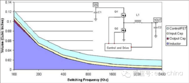
Figure 1.1 The size of the power supply component is mainly occupied by the semiconductor. The graph shows that the semiconductor volume does not change with frequency in nature, and this relationship may be too simplistic. There are two main types of semiconductor-related losses: conduction losses and switching losses. The conduction losses in synchronous buck converters are inversely proportional to the die area of ​​the MOSFET. The larger the MOSFET area, the lower its resistance and conduction losses. The switching loss is related to the speed of the MOSFET switch and how much input and output capacitance the MOSFET has. These are all related to the size of the device. Large volume devices have slower switching speeds and more capacitance. Figure 1.2 shows the relationship between two different operating frequencies (F). The conduction loss (Pcon) is independent of the operating frequency, while the switching losses (Psw F1 and Psw F2) are proportional to the operating frequency. Therefore, a higher operating frequency (Psw F2) results in higher switching losses. When the switching loss and conduction loss are equal, the total loss per operating frequency is the lowest. In addition, as the operating frequency increases, the total loss will be higher. However, at higher operating frequencies, the optimal die area is smaller, resulting in cost savings. In fact, at low frequencies, minimizing losses by adjusting the die area results in a very costly design. However, after moving to a higher operating frequency, we can optimize the die area to reduce losses, thereby reducing the semiconductor footprint of the power supply. The downside to this is that if we don't improve semiconductor technology, power efficiency will decrease.
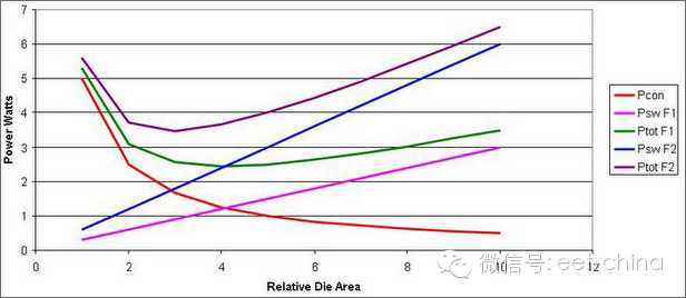
Figure 1.2 Increasing the operating frequency results in higher overall losses. As mentioned earlier, a higher operating frequency reduces the inductor volume; the required inner core plate is reduced. Higher frequencies also reduce the need for output capacitance. With ceramic capacitors, we can use lower capacitance values ​​or less. This helps to reduce the area of ​​the semiconductor die, which in turn reduces costs.
Tip 2: Driving noise power The noise-free power supply is not accidentally designed. A good power layout is designed to minimize experiment time. Taking minutes or even hours to look at the power layout carefully can save you days of troubleshooting time. Figure 2.1 shows the block diagram of some of the main noise-sensitive circuits inside the power supply. The output voltage is compared to a reference voltage to generate an error signal, which is then compared to a ramp to generate a PWM (Pulse Width Modulation) signal for driving the power stage. Power supply noise comes mainly from three places: error amplifier input and output, reference voltage, and ramp. Careful electrical and physical design of these nodes helps minimize troubleshooting time. In general, noise is capacitively coupled to these low level circuits. An excellent design ensures tight layout of these low level circuits and away from all switching waveforms. The ground plane also has a shielding effect.
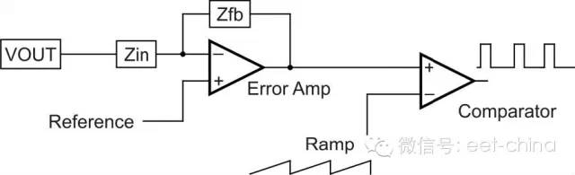
Figure 2.1. Many Noise Forming Opportunities for Low-Level Control Circuits The error amplifier input may be the most sensitive node in the power supply because it typically has the most connected components. If you combine it with the extremely high gain and high impedance of this stage, you will have endless troubles. During the layout process, you must minimize the length of the node and place the feedback and input components close to the error amplifier as close as possible. If there is a high frequency integrating capacitor in the feedback network, you must place it close to the amplifier and the other feedback components follow. Also, a series resistor-capacitor may also form a compensation network. The most ideal result is to place the resistor close to the input of the error amplifier, so that if a high-frequency signal is injected into the resistor-capacitor node, then the high-frequency signal has to withstand a higher resistance impedance - and the capacitor has a high-frequency signal The impedance is small. Slopes are another potential source of noise problems. The ramp is typically generated by capacitor charging (voltage mode) or by sampling (current mode) from the power switch current. In general, the voltage mode ramp is not a problem because the impedance of the capacitor to the high frequency injected signal is small. Current ramps are tricky because of rising edge peaks, relatively small ramp amplitudes, and power stage parasitics. Figure 2.2 shows some of the problems with current ramps. The first image shows the rising edge peak and the resulting current ramp. The comparators (depending on their speed) have two potential trip points, and the result is an out-of-order control that sounds more like a fried bacon. This problem can be well solved by using rising edge blanking in the control IC, which ignores the initial portion of the current waveform. The high frequency filtering of the waveform also helps to solve this problem. Also place the capacitor as close as possible to the control IC. As these two waveforms show, another common problem is subharmonic oscillation. This wide-narrow drive waveform appears to be insufficient slope compensation. Adding more voltage ramps to the current ramp will solve the problem.
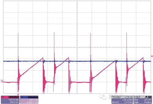

Figure 2.2 Two Common Current Mode Noise Problems Although you have designed the power layout quite carefully, there is still noise in your prototype power supply. What should I do? First, you have to make sure there is no problem with the loop response that eliminates the instability. Interestingly, the noise problem may look like instability at the crossover frequency of the power supply. But the real situation is that the loop is correcting the injection error with its fastest response speed. Again, the best approach is to identify that noise is being injected into one of three places: the error amplifier, the reference voltage, or the ramp. You only need to solve it step by step! The first step is to check the nodes to see if there is significant nonlinearity in the ramp or if there is a high frequency change in the error amplifier output. If no problems are found after the inspection, the error amplifier is removed from the circuit and replaced with a clean voltage source. This way you should be able to change the output of this voltage source to smoothly change the power output. If this works, then you have narrowed the problem down to the reference voltage and error amplifier. Sometimes, the reference voltage in the control IC is susceptible to the switching waveform. This situation may be improved by adding more (or appropriate) bypasses. In addition, using a gate drive resistor to slow down the switching waveform may also help to solve this problem. If the problem is with the error amplifier, it can be helpful to reduce the compensation component impedance as this reduces the amplitude of the injected signal. If all of these methods do not work, then the error amplifier node is removed from the printed circuit board. Air wiring the compensation components helps us identify where there is a problem.
Tip 3: Damped Input Filters Switching regulators are generally preferred over linear regulators because they are more efficient and the switching topology relies heavily on the input filter. This circuit component, combined with the typical negative dynamic impedance of the power supply, can induce oscillation problems. This article will explain how to avoid such problems. In general, all power supplies maintain their efficiency over a given input range. Therefore, the input power is more or less constant with the input voltage level. Figure 3.1 shows the characteristics of a switching power supply. As the voltage drops, the current continues to rise.
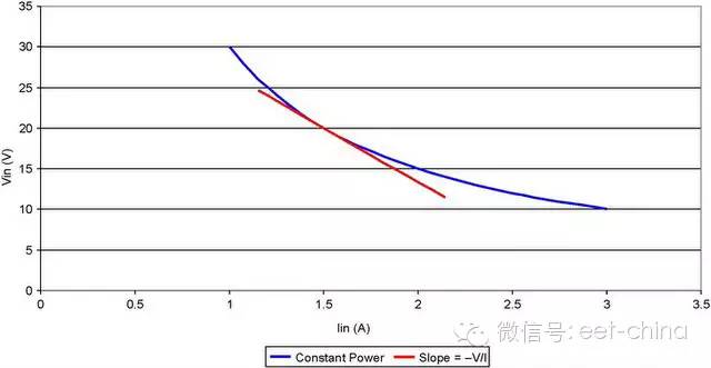
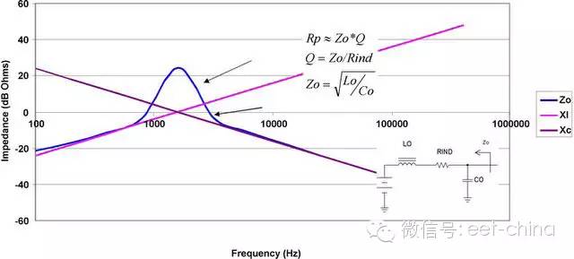

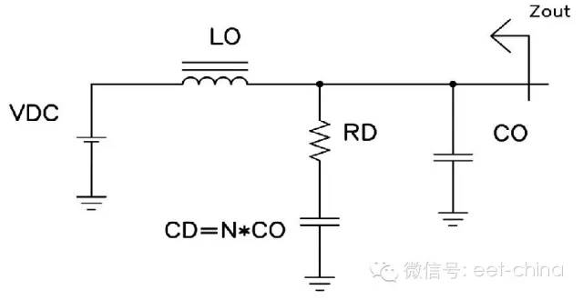
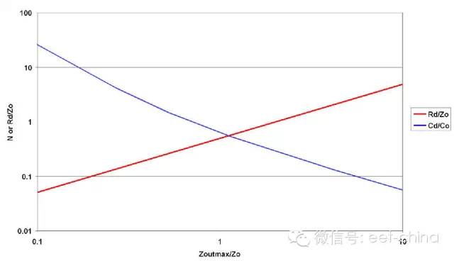
Controlling the source impedance at the front, we discuss how the source impedance of the input filter becomes resistive and how it interacts with the negative input impedance of the switching regulator. In extreme cases, these impedance amplitudes can be equal, but their signs are opposite to form an oscillator. A common standard in the industry is that the source impedance of the input filter should be at least 6 dB lower than the input impedance of the switching regulator as a safety margin to minimize the probability of oscillation. The input filter design typically begins with the selection of the input capacitor (CO shown in Figure 4.1) based on the ripple current rating or hold requirements. The second step typically involves selecting the inductor (LO) based on the EMI requirements of the system. As we discussed last month, near the resonance, the source impedance of these two components can be very high, resulting in system instability. Figure 1 depicts a method of controlling this impedance by placing a series resistor (RD) and a capacitor (CD) in parallel with the input filter. The filter can be damped with a resistor across the CO. However, in most cases, this will result in excessive power loss. Another method is to add a series connected inductor and resistor across the filter inductor.

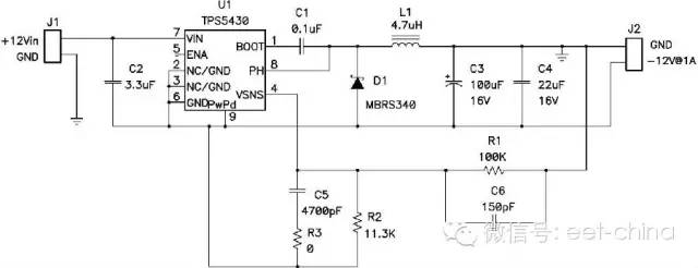
Tip 4: The use of buck controllers in boost power design electronic circuits typically operate at a positive regulated output voltage, which is typically provided by a buck regulator. If a negative output voltage is also required, the same buck controller can be configured in a buck-boost topology. Negative Output Voltage Buck-Boost is sometimes referred to as a negative inversion with an operating duty cycle of 50%, which provides an output voltage equivalent to the input voltage but opposite in polarity. It can adjust the duty cycle as the input voltage fluctuates, maintaining the regulation with a “buck†or “boost†output voltage. Figure 5.1 shows a thin buck-boost circuit with the switching voltage present on the inductor. In this way, the similarity between the circuit and the standard buck converter will suddenly become clear. In fact, it is exactly the same as the buck converter except that the output voltage is the opposite of the ground. This layout can also be used for synchronous buck converters. This is similar to the buck or synchronous buck converter side because it operates differently than a buck converter. The voltage appearing on the inductor when the FET is switched is different from the voltage of the buck converter. As in buck converters, it is necessary to balance the volt-microsecond (V-μs) product to prevent inductor saturation. When the FET is on (as in the ton interval shown in Figure 1), all input voltage is applied to the inductor. A positive voltage on the "point" side of the inductor causes the current to ramp up, which results in the product's turn-on time V-μs product. During the FET turn-off (toff), the voltage polarity of the inductor must be reversed to maintain the current so that the pull side is negative. The inductor current ramps down and flows through the load and output capacitors and back through the diode. The V-μs product when the inductor is turned off must be equal to the V-μs product at turn-on. Since Vin and Vout are unchanged, it is easy to derive the expression for the duty cycle (D): D = Vout / (Vout " Vin). This control circuit maintains the output voltage by calculating the correct duty cycle. Voltage regulation. Both the above expression and the waveform shown in Figure 5.1 are assumed to operate in continuous conduction mode.

Tip 5: Accurate Measurement of Power Supply Ripple Accurately measuring power supply ripple is an art in itself. In the example shown in Figure 6.1, a junior engineer completely misused an oscilloscope. His first mistake was to use an oscilloscope probe with a long ground lead; his second mistake was to place the loop and ground lead formed by the probe near the power transformer and switching components; his last One mistake is to allow excess inductance between the oscilloscope probe and the output capacitor. This problem appears as a high frequency pick in the ripple waveform. In the power supply, there are a large number of high-speed, large-signal voltage and current waveforms that can be easily coupled to the probe, including the magnetic field coupled from the power transformer, the electric field coupled from the switching node, and the common mode generated by the transformer's inter-winding capacitor. Current.

Figure 6.1 Poor measurement results from incorrect ripple measurements The correct measurement method can greatly improve the measured ripple results. First, bandwidth limitations are often used to specify ripple to prevent picking up high frequency noise that is not really present. We should set the correct bandwidth limit for the oscilloscope used for the measurement. Second, by removing the probe "cap" and constructing a pickup (as shown in Figure 6.2), we can eliminate the antenna formed by the long ground lead. Wrap a small length of wire around the probe ground connection point and connect the ground to the power source. This can reduce the length of the tip exposed to high electromagnetic radiation near the power supply, further reducing pickup. Finally, in an isolated power supply, a large amount of common mode current flows through the probe ground connection point. This creates a voltage drop between the power ground connection point and the oscilloscope ground connection point, which appears as ripple. To prevent this from happening, we need to pay special attention to the common mode filtering of the power supply design. In addition, winding the oscilloscope leads around the ferrite core also helps to minimize this current. This results in a common-mode inductor that reduces the measurement error caused by the common-mode current while not affecting the differential voltage measurement. Figure 6.2 shows the ripple voltage for this identical circuit, which uses an improved measurement method. In this way, the high frequency peak is really eliminated.

Figure 6.2 Four minor changes greatly improve the measurement results. In fact, after integration into the system, the power supply ripple performance is even better. There is almost always some inductance between the power supply and other components of the system. This inductance may be present in the wiring, or only the etching is present on the PWB. In addition, there is always an extra bypass capacitor around the chip, which is the load on the power supply. Together, these form a low pass filter that further reduces power supply ripple and/or high frequency noise. In extreme cases, the cutoff frequency of the filter is 400 kHz when the current flows through a one-inch conductor of 15nH inductor and 10μF bypass capacitor for a short time. In this case, it means that the high frequency noise will be greatly reduced. In many cases, the filter's cutoff frequency will be below the power supply ripple frequency, potentially reducing ripple significantly. Experienced engineers should be able to find ways to use this approach during their testing.
Tip 6: Efficiently driving LED off-line lighting It may take years to replace incandescent light bulbs with practical screw-in LEDs, and the use of LEDs in architectural lighting is growing, with higher reliability and Energy saving potential. Like most electronics, it requires a power supply to convert input power into a form that LEDs can use. In streetlight applications, one possible configuration is to create 80 series LEDs with 300V/0.35 amp load. Isolation and Power Factor Correction (PFC) requirements are required when selecting a power supply topology. Isolation requires a large number of safety trade-offs, including the trade-off between the need for shock protection and the complexity of power supply design. In this application, there is a high voltage on the LED. It is generally considered that isolation is not necessary, and PFC is required, because the lighting of more than 25 watts in Europe requires PFC function, and this product is launched for the European market. . For this application, there are three alternative power supply topologies: buck topology, transfer mode reverse topology, and transfer mode (TM) single-ended primary inductor converter (SEPIC) topology. The buck topology can be used very efficiently to meet harmonic current requirements when the LED voltage is approximately 80 volts. In this case, the higher load voltage will no longer be able to use the buck topology. Then, the compromise is to use reverse topology and SEPIC topology. The SEPIC has the advantage that it clamps the switching waveform of the power semiconductor device, allowing the use of lower voltages, making the device more efficient. In this application, an efficiency increase of approximately 2% can be obtained. In addition, there are fewer rings in the SEPIC, making EMI filtering easier. Figure 7.1 shows the schematic of this power supply.
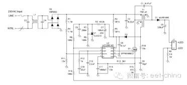
Figure 7.1 Transfer Mode SEPIC acts as a simple LED driver. The circuit uses a boost TM PFC controller to control the input current waveform. The circuit begins with off-line charging for C6. Once started, the controller's power supply is provided by an auxiliary winding on the SEPIC inductor. A relatively large output capacitor limits the LED ripple current to 20% of the DC current. In addition, the AC flux and current in the TM SEPIC are very high, requiring lacquered strands and low loss inner core plates to reduce inductance losses. Figure 7.2 and Figure 7.3 show the experimental results of the prototype circuit that matches the schematic in Figure 7.1. Compared with the European line range, its efficiency is very high, up to 92%. This high efficiency is achieved by limiting ringing on the power device. Also, as we can see from the current waveform, the power factor is very good above 96% efficiency. Interestingly, the waveform is not a pure sinusoid, but rather has some slope on the rising and falling edges. This is because the circuit does not measure the input current and only measures the switching current. However, this waveform is still sufficient to pass the European harmonic current requirements.
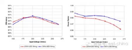
Figure 7.2 TM SEPIC has good efficiency and high PFC efficiency
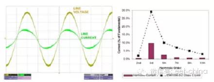
Figure 7.3 Line current easily passes the EN61000-3-2 Class C standard
Tip 7: Reduce EMI performance by changing the power frequency. When measuring EMI performance, did you find that no matter what method you use, there are still problems that exceed the specification by a few dB? There is a way to help you meet EMI performance requirements or simplify your filter design. This approach involves modulation of the power switching frequency to introduce sideband energy and to change the narrowband noise to wideband emission characteristics to effectively attenuate harmonic peaks. It should be noted that the overall EMI performance has not been reduced, but has been redistributed. With sinusoidal modulation, the two variables of the controllable variable are the modulation frequency (fm) and the magnitude of the power switching frequency (Δf) that you change. The modulation index (Β) is the ratio of these two variables: 
Figure 8.1 shows the effect of changing the modulation index by a sine wave. When Β = 0, there is no frequency shift, only one line. When Β = 1, the frequency feature begins to extend and the center frequency component drops by 20%. When Β = 2, the feature will extend further and the maximum frequency component is 60% of the initial state. Frequency modulation theory can be used to quantify the amount of energy in the spectrum. The Carson rule states that most of the energy will be contained in the 2 * (Δf + fm) bandwidth.
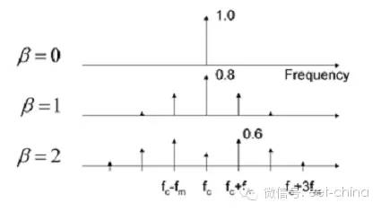
Figure 8.1 Modulated Power Switching Frequency Extends EMI Characteristics
Figure 8.2 shows a larger modulation index and shows that it is possible to reduce peak EMI performance above 12 dB.
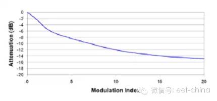
Figure 8.2 Larger Modulation Index Can Further Reduce Peak EMI Performance
Choosing the modulation frequency and frequency shift are two very important aspects. First, the modulation frequency should be higher than the EMI receiver bandwidth so that the receiver does not measure both sidebands at the same time. However, if the frequency you choose is too high, the power control loop may not be able to fully control this change, resulting in a change in output voltage at the same rate. In addition, this modulation can cause audible noise in the power supply. Therefore, the modulation frequency we choose cannot generally be much higher than the receiver bandwidth, but greater than the audible noise range. Obviously, we can see from Figure 8.2 that it is preferable to change the working frequency a lot. However, this will affect the power supply design and it is very important to realize this. That is, the magnetic element is selected for the lowest operating frequency. In addition, the output capacitors need to handle the larger ripple currents associated with lower frequency operation. Figure 8.3 compares EMI performance measurements with frequency modulation and no frequency modulation. At this point the modulation index is 4, and as we expected, the EMI performance at the fundamental frequency is reduced by approximately 8 dB. Other aspects are also important. The harmonics are smear into the frequency band corresponding to their number, ie the third harmonic extends to three times the fundamental frequency. This situation is repeated at some higher frequencies, resulting in a noise floor that is much higher than the fixed frequency. Therefore, this method may not be suitable for low noise systems. However, many systems have benefited from this approach by increasing design margins and minimizing EMI filter costs.
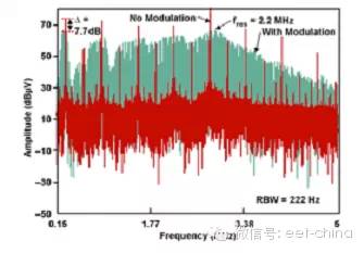
Figure 8.3 Changing the power frequency reduces the fundamental frequency but increases the noise floor
Tip #8: Estimating the Temperature Rise of Surface Mount Semiconductors In the past, estimating the temperature rise of semiconductors is very simple. You only need to calculate the power consumption of the component, and then use the cooling circuit electrical simulation to determine the type of heat sink required. This problem is now complicated by the desire to remove heat sinks due to size and cost considerations. Semiconductors placed in a thermally enhanced package require a board that acts as a heat sink and provides all the necessary cooling. As shown in Figure 9.1, heat flows into the printed circuit board (PWB) through a metal mounting sheet and package. The heat then flows from the side through the PWB trace and diffuses through the surface of the board through the natural convection into the surrounding environment. An important factor affecting the temperature rise of the die is the copper content in the PWB and the surface area for convective heat conduction.

Figure 9.1 Heat flows from the side through the PWB trace and then from the PWB surface to the surrounding environment. The semiconductor product specification usually lists the thermal resistance of the junction from the PWB structure to the surrounding environment. This means that designers can calculate the temperature rise by simply multiplying this thermal resistance by the power dissipation. However, if the design does not have a specific structure, or if it is necessary to further reduce the thermal resistance, then many problems will arise. Figure 9.2 shows a simplified electrical simulation of the heat flow problem, which we can analyze in depth. The IC power supply is represented by a current source and the thermal resistance is represented by a resistor. The circuit is solved at various voltages, which provides a simulation of the temperature. There is thermal resistance from the junction to the mounting surface, while the lateral resistance across the board and the resistance of the board surface to the surrounding environment together form a ladder network. This model assumes that 1) the board is mounted vertically, 2) there is no forced convection or radiant cooling, all heat flows in the copper of the board, and 3) there is almost no temperature difference on either side of the board.

Figure 9.2 Thermal Flow Electrical Equivalence Simplifies Temperature Rise Estimation Figure 9.3 shows the effect of increasing copper content in PWB on thermal resistance. Increasing 1.4 mils of copper (two-sided, half-ounce) to 8.4 mils (4 layers, 1.5 ounces) increases the thermal resistance by a factor of three. The two curves in the figure are: a small package with a diameter of 0.2 inches representing heat flow into the board; and a large package with a diameter of 0.4 inches representing heat flow into the board. Both curves are for a 9 square inch PWB. Both of these curves are closely related to the nominal data and both help to estimate the impact of changing the board structure of the product specification. But you need to be cautious when using this data, which assumes no other power consumption in the 9 square inch PWB, but it is not.

Figure 9.3 Thermal Flow Electrical Equivalence Simplifies Temperature Rise Estimation Techniques Nine: Easily Estimate Load Transient Response This power supply design tip describes an easy way to estimate the transient response of a power supply by understanding the control bandwidth and output filter capacitance characteristics. This method takes full advantage of the fact that the closed-loop output impedance of all circuits is the open-loop output impedance divided by 1 plus the loop gain, or simply expressed as: 
Figure 10.1 graphically illustrates the above relationship, both impedances being in dB-Ω or 20*log [Z]. In the low frequency region on the open loop curve, the output impedance is dependent on the output inductor impedance and inductance. When the output capacitor and the inductor resonate, a peak is formed. The high frequency impedance is dependent on the capacitance output filter characteristics, equivalent series resistance (ESR), and equivalent series inductance (ESL). The closed-loop output impedance can be calculated by dividing the open-loop impedance by 1 plus the loop gain. Since the graph is expressed in logarithm, that is, simple subtraction, the impedance is greatly reduced in the low frequency region where the gain is high; the closed loop and open loop impedance are substantially the same in the high frequency region where the gain is small. The following points need to be explained here: 1) the peak loop impedance appears near the power crossover frequency, or where the loop gain is equal to 1 (or 0 dB); and 2) most of the time, the power control bandwidth will Higher than the filter resonance, so the peak closed-loop impedance will depend on the output capacitor impedance at the crossover frequency.
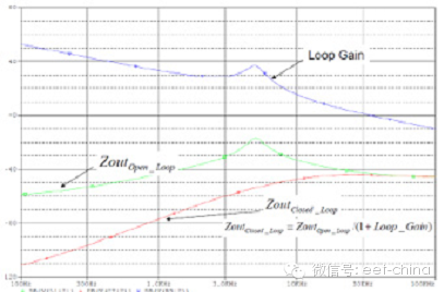
Figure 10.1 Closed-loop output impedance peak Zout appears at the control loop crossover frequency Once the peak output impedance is known, the transient response can be easily estimated by the product of the load variation and the peak closed-loop impedance. There are a few caveats to note. Since the low phase margin causes peaking, the actual peak value may be higher. However, for rapid estimation, this effect is negligible [1]. The second thing to note is related to the increase in load variation. If the magnitude of the load change is slow (dI/dt is low), the response depends on the closed-loop output impedance of the low-frequency region associated with the rise time; if the magnitude of the load change is extremely fast, the output impedance will depend on the output filter ESL. If this is the case, more high frequency bypass may be required. Finally, in the case of very high performance systems, the power stage of the power supply may limit the response time, ie the current in the inductor may not respond as quickly as the control loop expects because the inductor and applied voltage limit the current. Conversion rate. Below is an example of how to use the above relationship. The problem is to pick an output capacitor based on a 50mV output change within the allowable range of the 10kHz variation of the 200kHz switching power supply. The allowed peak output impedance is: Zout = 50mV/10 amps or 5 milliohms. This is the maximum allowable output capacitor ESR. The next step is to build the required capacitance. Fortunately, both ESR and capacitors are orthogonal and can be handled separately. An Aggressive power control loop bandwidth can be 1/6 or 30 kHz of the switching frequency. Therefore, the output filter capacitor at 30 kHz requires a reactance of less than 5 milliohms, or a capacitance higher than 1000uF. Figure 10.2 shows the load transient simulation for this problem with a 5 milliohm ESR, 1000uF capacitor, and 30kHz voltage mode control conditions. The output voltage changes approximately 52 mV in terms of the 10 amp load variation that verifies that this method is valid.

Figure 10.2 Simulation Verification Estimating Load Transient Performance
Tip #10: Easily Estimate Solving Power Circuit Loss Problems Have you calculated the estimated component losses in the design in detail, but found that there is a big difference between the measured results and the laboratory measurements? This power supply design tip describes an easy way to help you eliminate the difference between calculated and actual measurements. The method is based on the Taylor series expansion, where it is specified (under a given free condition) that any function can be decomposed into a polynomial, as follows: 
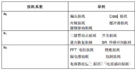
If you realize that the power loss is related to the output current (the output current can be replaced by X), the coefficient term can be well correlated with the power loss of the source from different sources. For example, ao represents a fixed overhead loss such as gate drive, bias supply and core, and losses such as power transistor Coss charging and discharging. These losses are independent of the output current. The second associated loss, a1, is directly related to the output current, which is typically characterized by output diode losses and switching losses. In the output diode, most of the losses are due to the junction voltage, so the losses increase proportionally with the output current. Similarly, switching losses can be approximated by the product of the output current correlation term and some fixed voltage. The third item is easily identified as conduction loss. Typical performance is the loss in FET resistance, magnetic wiring resistance, and interconnect resistance. Higher order terms may be useful in calculating nonlinear losses such as core losses. Useful results can only be obtained by considering the first three cases. One way to calculate the three coefficients is to measure the losses at three operating points and solve the results in a matrix. This solution can be simplified if one of the loss measurements is obtained under no-load conditions (ie, all losses are equal to the first coefficient a0). The problem is then reduced to two equations and two unknowns that are easy to solve. Once the coefficients are calculated, a loss curve similar to Figure 11.1 showing three loss types can be constructed. This curve is useful in eliminating deviations between measurement results and calculation results, and helps to identify potential areas where efficiency can be improved. For example, under full load conditions, the losses in Figure 1 are primarily conduction losses. To increase efficiency, you need to reduce FET resistance, inductive resistance, and interconnect resistance.

Figure 11.1: The power loss component matches the quadratic coefficient. The correlation between the actual loss and the trinomial is very good. Figure 11.2 compares the measured data of the synchronous buck regulator with the curve fit data. We know that there will be three coincident points on the curve based on solving three simultaneous equations. For the remainder of the curve, the difference between the two curves is less than 2%. Other types of power supplies may be difficult to match because of different operating modes (such as continuous or non-continuous), pulse hopping, or variable frequency operation. This approach is not absolutely reliable, but it helps the power supply designer understand the actual circuit losses.
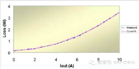
Figure 11.2 The first three loss terms provide a good correlation with the measured values.
Finally: Power Efficiency Maximization In the previous section, we discussed how to use Taylor series to find sources of loss in the power supply. In this power supply design technique, we will discuss how to use the same number of stages to maximize the power efficiency of a particular load current. In the previous section, we recommend using the following output current function to calculate the power loss: 
The next step is to take advantage of the simple expression above and put it into the efficiency equation: 
In this way, the efficiency of the output current is optimized (the specific demonstration work is left to the students to complete). This optimization can produce an interesting result. When the output current is equal to the following expression, the efficiency will be maximized. 
The first thing to note is that the a1 term has no effect on the current when the efficiency is at its maximum. This is because it is related to loss, which in turn is proportional to the output current, such as the diode junction. Therefore, as the output current increases, the above loss and output power also increase, and there is no effect on efficiency. The second thing to note is that the best efficiency occurs at some point where the fixed loss and the conduction loss are equal. That is to say, as long as the components that set the values ​​of a0 and a2 are controlled, the best efficiency can be obtained. Still try to reduce the value of a1 and improve efficiency. The result of controlling this is the same for all load currents, so the best efficiency does not occur as with other items. The goal of item a1 is to minimize costs while controlling costs. Table 1 summarizes the various power loss terms and their associated loss factors. This table provides some compromises in optimizing power efficiency. For example, the choice of power MOSFET on-resistance affects its gate drive requirements and Coss losses and potential buffer losses. Low on-resistance means that gate drive, Coss, and buffer losses increase inversely. Therefore, you can control a0 and a2 by selecting the MOSFET. Table 1 Loss factor and corresponding power loss
Algebraic next generation returns the optimal current back to the efficiency equation, and the maximum efficiency is solved: the last two of the expressions need to be minimized to optimize efficiency. The a1 item is very simple, just minimize it. The last item can be partially optimized. If the MOSFET's Coss and gate drive power are assumed to be related to their area and their on-resistance is inversely proportional to the area, then the optimum area (and resistance) can be chosen for it. Figure 12.1 shows the optimization results for the die area. When the die area is small, the on-resistance of the MOSFET becomes an efficiency limiter. As the die area increases, the drive and Coss losses increase. 
Figure 12.1 Adjusting MOSFET Die Area to Minimize Full Load Power Loss Figure 12.2 is a three possible design efficiency plot around the best point in Figure 12.1. The normal die area for the three designs is shown separately.轻负载情况下,较大é¢ç§¯è£¸ç‰‡çš„效率会å—ä¸æ–å¢žåŠ çš„é©±åŠ¨æŸè€—å½±å“,而在é‡è´Ÿè½½æ¡ä»¶ä¸‹å°å°ºå¯¸å™¨ä»¶å› é«˜ä¼ å¯¼æŸè€—而å˜å¾—ä¸å ªé‡è´Ÿã€‚这些曲线代表裸片é¢ç§¯å’Œæˆæœ¬çš„三比一å˜åŒ–,注æ„这一点éžå¸¸é‡è¦ã€‚æ£å¸¸èŠ¯ç‰‡é¢ç§¯è®¾è®¡çš„效率åªæ¯”满功率大é¢ç§¯è®¾è®¡çš„效率ç¨ä½Žä¸€ç‚¹ï¼Œè€Œåœ¨è½»è½½æ¡ä»¶ä¸‹ï¼ˆè®¾è®¡å¸¸å¸¸è¿è¡Œåœ¨è¿™ç§è´Ÿè½½æ¡ä»¶ä¸‹ï¼‰åˆ™æ›´é«˜ã€‚

图12.2 效率峰值出现在满é¢å®šç”µæµä¹‹å‰
Welding diodes are available for medium frequency (over 2KHz) and high frequency (over 10khz) applications.They have very low on - state voltage and thermal resistance. Welding diodes are designed for medium and high frequency welding equipment and optimized for high current rectifiers. The on-state voltage is very low and the output current is high.
Welding Diode,Disc Welding Diode,3000 Amp Welding Diode,High Current Rectifier Welding Diode
YANGZHOU POSITIONING TECH CO., LTD. , https://www.cnchipmicro.com