IGBT (Insulated Gate Bipolar Transistor), insulated gate bipolar transistor, is a composite fully controlled voltage-driven power semiconductor device composed of BJT (bipolar transistor) and MOS (insulated gate field effect transistor), which has both MOSFETs. The advantages of both the high input impedance and the low turn-on voltage drop of the GTR. The GTR saturation voltage is reduced, the current carrying density is large, but the driving current is large; the MOSFET driving power is small, the switching speed is fast, but the conduction voltage drop is large, and the current carrying density is small. The IGBT combines the advantages of the above two devices, with low driving power and reduced saturation voltage. It is very suitable for converter systems with DC voltages of 600V and above, such as AC motors, inverters, switching power supplies, lighting circuits, traction drives, etc.
Before the development of insulated gate bipolar transistors (IGBTs), power FET MOSFETs were used in medium and low voltage applications where fast switching was required. Thyristors and GTOs were used in the medium and high voltage fields. Although the MOSFET has the advantages of fast switching speed, high input impedance, good thermal stability, and simple driving circuit, the on-resistance of the MOSFET increases rapidly with the increase of the breakdown voltage at 200V or higher. The power consumption is greatly increased, and there are defects in that high withstand voltage and large-capacity components cannot be obtained. The bipolar transistor has excellent low forward voltage drop characteristics, and although a high withstand voltage and large capacity component can be obtained, it requires a large driving current, a complicated control circuit, and a fast switching speed.
IGBT was developed to meet this requirement. It is a device composed of a MOSFET (input stage) and a PNP transistor (output stage). It has the characteristics of small driving power and fast switching speed of the MOSFET device (control) And response), there are bipolar devices with reduced saturation voltage and large capacity (power level is more durable), frequency characteristics between the MOSFET and the power transistor, can work normally in the frequency range of tens of KHz. Based on these excellent characteristics, IGBTs have been widely used in applications with voltages exceeding 300V. Modular IGBTs can meet higher current conduction requirements, and their applications continue to increase, and there will be even greater development in the future.
IGBT structure and characteristics:
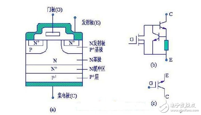
As shown in the figure, an N-channel reinforced insulated gate bipolar transistor structure, the N+ region is referred to as a source region, and the electrode attached thereto is referred to as a source (ie, emitter E). The N base is called the drain area. The control region of the device is the gate region, and the electrode attached thereto is called the gate (ie, gate G). The channel is formed next to the boundary of the gate region. The P-type region (including the P+ and P-regions) between the C and E poles (the channel is formed in this region) is called a Subchannel region. The P+ region on the other side of the drain region is called a drain injector. It is a unique functional region of the IGBT. Together with the drain region and the sub-channel region, a PNP bipolar transistor is formed to function as an emitter. The drain injects holes and conducts conductive modulation to lower the on-state voltage of the device. The electrode attached to the drain implant region is referred to as the drain (ie, collector C).
The switching function of the IGBT is to form a channel by adding a forward gate voltage, and provide a base current to the PNP (formerly NPN) transistor to turn on the IGBT. Conversely, the reverse gate voltage is applied to eliminate the channel, and the base current is cut off to turn off the IGBT. The driving method of the IGBT is basically the same as that of the MOSFET, and it only needs to control the input pole N-channel MOSFET, so it has high input impedance characteristics. When the channel of the MOSFET is formed, the hole from the P+ base is injected into the N-layer (small sub-), and the N-layer is conductance modulated to reduce the resistance of the N-layer, so that the IGBT also has a low voltage at a high voltage. On-state voltage.
The IGBT is a composite switching device that combines MOSFET and GTR technology. It is formed by adding a p+ layer to the drain of the power MOSFET. The performance is also combined with the advantages of MOSFET and bipolar power transistor. The N+ region is referred to as the source region, and the electrode attached thereto is referred to as the source (i.e., emitter E). The P+ zone is called the drain zone. The control region of the device is the gate region, and the electrode attached thereto is called the gate (ie, gate G). The channel is formed next to the boundary of the gate region. The P-type region (including the P+ and P-regions) between the C and E poles (the channel is formed in this region) is called a Subchannel region. The P+ region on the other side of the drain region is called a drain injector. It is a unique functional region of the IGBT. Together with the drain region and the sub-channel region, a PNP bipolar transistor is formed to function as an emitter. The drain injects holes and conducts conductive modulation to reduce the on-state voltage drop of the device. The electrode attached to the drain implant region is referred to as the drain (ie, collector C).
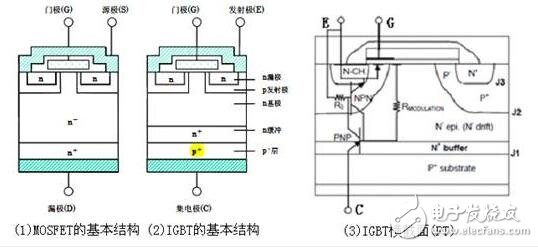
The IGBT is composed of an N-channel MOSFET and a PNP-type GTR. It is actually a composite tube with a GTR as the leading component and a MOSFET as the driving component. In addition to the PNP transistor structure, the IGBT also has an NPN transistor structure that is turned off by shorting its base and emitter to the source metal terminal of the MOSFET. The 4-layer PNPN structure of the IGBT, the built-in PNP and the NPN transistor form a thyristor structure, which may cause the IGBT's pillar effect. Unlike MOSFETs, IGBTs do not have parasitic reverse diodes inside, so in practical use (inductive loads), a suitable fast recovery diode is required.
The ideal equivalent circuit and actual equivalent of IGBT are shown in the figure :
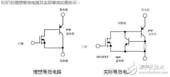
Ideal equivalent circuit and actual equivalent circuit of IGBT
The IGBT can be used as a monolithic Bi-MOS transistor formed by Darlington connection of a PNP bipolar transistor and a power MOSFET by an equivalent circuit.
Therefore, when a positive voltage is applied between the gate and the emitter to turn on the power MOSFET, the base-collector of the PNP transistor is connected with a low resistance, thereby turning the PNP transistor on, due to passing through the drain. By adding a p+ layer, a hole is injected from the p+ layer to the n base in an on state, thereby causing a transition in conduction performance, so that it can obtain an extremely low on-state resistance as compared with a power MOSFET.
Thereafter, when the voltage between the gate and the emitter is 0 V, first, the power MOSFET is in an open state, and the base current of the PNP transistor is cut off, thereby being in an open state.
As mentioned above, the IGBT is the same as the power MOSFET, and the turn-on and turn-off actions can be controlled by the voltage signal.
Operating characteristics of IGBT:
Static characteristics
The static characteristics of IGBTs mainly include volt-ampere characteristics, transfer characteristics and switching characteristics.
The volt-ampere characteristic of the IGBT is the relationship between the drain current and the gate voltage when the gate-source voltage Ugs is used as a parameter. The output drain current is controlled by the gate-source voltage Ugs. The higher the Ugs, the larger Id. It is similar to the output characteristics of GTR. It can also be divided into a saturated zone 1, an enlarged zone 2, and a breakdown characteristic 3 part. In the off-state IGBT, the forward voltage is taken over by the J2 junction and the reverse voltage is taken up by the J1 junction. If there is no N+ buffer, the forward and reverse blocking voltage can be achieved at the same level. After the N+ buffer is added, the reverse shutdown voltage can only reach tens of volts, thus limiting the application range of the IGBT.
The transfer characteristic of the IGBT is a relationship between the output drain current Id and the gate-source voltage Ugs. It has the same transfer characteristics as the MOSFET. When the gate-source voltage is less than the turn-on voltage Ugs(th), the IGBT is turned off. Id is linear with Ugs over most of the drain current range after the IGBT is turned on. The maximum gate-to-source voltage is limited by the maximum drain current, and the optimum value is generally about 15V.
The switching characteristics of the IGBT refer to the relationship between the drain current and the drain-source voltage. When the IGBT is in the on state, its PNP transistor is a wide base transistor, so its B value is extremely low. Although the equivalent circuit is a Darlington structure, the current flowing through the MOSFET becomes a major part of the total current of the IGBT. At this time, the on-state voltage Uds(on) can be expressed by the following formula:
Uds(on) = Uj1 + Udr + IdRoh
Where Uj1 is the forward voltage of the JI junction, which is 0.7 to 1V; Udr is the voltage drop across the extended resistor Rdr; Roh is the channel resistance.
The on-state current Ids can be expressed by:
Ids=(1+Bpnp)Imos
Where Imos is the current flowing through the MOSFET.
Due to the conductance modulation effect in the N+ region, the on-state voltage drop of the IGBT is small, and the on-state voltage drop of the IGBT with a withstand voltage of 1000V is 2 to 3V. When the IGBT is in the off state, only a small leakage current exists.
2. Dynamic characteristics
During the turn-on process, the IGBT is operated as a MOSFET most of the time, except that after the drain-source voltage Uds falls, the PNP transistor is amplified from the amplification region to a delay time. Td(on) is the turn-on delay time and tri is the current rise time. The drain current turn-on time ton, which is often given in practical applications, is the sum of td (on) tri . The falling time of the drain-source voltage consists of tfe1 and tfe2.
The triggering and turn-off of the IGBT requires a forward voltage and a negative voltage between the gate and the base. The gate voltage can be generated by different drive circuits. When selecting these driver circuits, they must be based on the following parameters: device turn-off bias requirements, gate charge requirements, solidity requirements, and power conditions. Because the IGBT gate-emitter impedance is large, MOSFET drive technology can be used for triggering. However, since the input capacitance of the IGBT is larger than that of the MOSFET, the turn-off bias of the IGBT should be higher than that provided by many MOSFET drive circuits.
The switching speed of the IGBT is lower than that of the MOSFET, but it is significantly higher than the GTR. The IGBT does not require a negative gate voltage to turn off the turn-off time when turned off, but the turn-off time increases as the gate and emitter shunt resistance increases. The turn-on voltage of the IGBT is about 3 to 4V, which is equivalent to the MOSFET. The saturation voltage drop when the IGBT is turned on is lower than that of the MOSFET and is close to the GTR, and the saturation voltage drop decreases as the gate voltage increases.
The working principle of IGBT:
IGBTs are a natural evolution of vertical power MOSFETs for high current, high voltage applications and fast end devices. Since a higher breakdown voltage BVDSS requires a source-drain path, and this channel has a high resistivity, resulting in a power MOSFET having a high RDS(on) value, the IGBT eliminates these existing power MOSFETs. The main drawback. Although the latest generation of power MOSFET devices have greatly improved the RDS(on) characteristics, at high levels, the power conduction losses are still much higher than the IGBT technology. The lower voltage drop, the ability to convert to a low VCE (sat), and the structure of the IGBT, support higher current densities and simplify the schematic of the IGBT driver compared to a standard bipolar device.
The N-channel type IGBT operates by forming a (positive) voltage above the gate-emitter plus threshold voltage VTH, forming an inversion layer (channel) on the p layer directly under the gate electrode, starting from the emitter electrode. The lower n-layer injects electrons. This electron is a minority carrier of the p+np transistor, and flows into the hole from the p+ layer of the collector substrate to perform conductivity modulation (bipolar operation), so that the collector-emitter saturation voltage can be lowered. The equivalent circuit during operation is shown in Figure 1(b), and the symbol of the IGBT is shown in Figure 1(c). An n+pn-parasitic transistor is formed on the emitter electrode side. If the n+pn-parasitic transistor operates, it becomes a p+n-pn+ thyristor. The current continues to flow until the output side stops supplying current. Control is no longer possible by the output signal. This state is generally referred to as a latched state.
In order to suppress the operation of the n+pn-parasitic transistor, the current amplification factor α of the p+np transistor is minimized as a measure for solving the blocking. Specifically, the current amplification factor α of p+np is designed to be 0.5 or less. The blocking current IL of the IGBT is more than three times the rated current (DC). The driving principle of the IGBT is basically the same as that of the power MOSFET, and the on-off is determined by the gate emitter voltage uGE.
(1) Conduction
The structure of the IGBT silicon is very similar to that of the power MOSFET. The main difference is that the IGBT adds a P+ substrate and an N+ buffer layer (NPT-non-punch-IGBT technology does not add this part), one of the MOSFETs drives two bipolar devices. . The application of the substrate creates a J1 junction between the P+ and N+ regions of the tube. When the positive gate bias causes the P base region to be inverted below the gate, an N-channel is formed, a current flow occurs simultaneously, and a current is generated in exactly the manner of the power MOSFET. If the voltage generated by this electron current is in the range of 0.7V, then J1 will be in forward bias, some holes will be injected into the N-region, and the resistivity between the anode and cathode will be adjusted, which reduces power conduction. The total loss and the second charge flow is initiated. The net result is that two different current topologies appear temporarily in the semiconductor hierarchy: one electron current (MOSFET current) and hole current (bipolar). When uGE is greater than the turn-on voltage UGE(th), a channel is formed in the MOSFET to provide a base current for the transistor and the IGBT is turned on.
(2) On-voltage drop:
The conductance modulation effect reduces the resistance RN and makes the on-state voltage drop small.
(3) Shutdown:
When a negative bias is applied to the gate or the gate voltage is below the threshold, the channel is disabled and no holes are injected into the N-region. In any case, if the MOSFET current drops rapidly during the switching phase, the collector current gradually decreases because there are a small number of carriers (small sub-) in the N-layer after the commutation starts. This reduction in residual current value (wake) depends entirely on the density of the charge at turn-off, which in turn is related to several factors, such as the amount and topology of the dopant, the gradation thickness, and the temperature. The attenuation of the minority carriers causes the collector current to have a characteristic wake waveform, and the collector current causes the following problems: increased power consumption; cross conduction problems, especially in devices using freewheeling diodes, the problem is more pronounced.
In view of the fact that the wake is related to the reorganization of the minority, the current value of the wake should be closely related to the hole mobility closely related to the temperature, IC and VCE of the chip. Therefore, depending on the temperature reached, it is feasible to reduce the undesirable effects of this current on the design of the terminal device, which is related to VCE, IC and TC.
When a back pressure or no signal is applied between the gate emitters, the channel in the MOSFET disappears, the base current of the transistor is cut off, and the IGBT is turned off.
(4) Reverse blocking:
When a reverse voltage is applied to the collector, J1 is reverse biased and the depletion layer expands toward the N-region. This mechanism is important because it can't achieve an effective blocking ability because it reduces the thickness of this level too much. On the other hand, if the size of this area is excessively increased, the pressure drop is continuously increased.
(5) Forward blocking:
When the gate and emitter are shorted and a positive voltage is applied to the collector terminal, the P/NJ3 junction is controlled by the reverse voltage. At this time, the externally applied voltage is still withstood by the depletion layer in the N drift region.
(6) Latch:
The IGBT has a parasitic PNPN thyristor between the collector and the emitter. Under special conditions, this parasitic device will turn on. This phenomenon causes an increase in the amount of current between the collector and the emitter, a decrease in the controllability of the equivalent MOSFET, and usually causes a breakdown of the device. The thyristor conduction phenomenon is called IGBT latching. Specifically, the causes of such defects are different from each other and are closely related to the state of the device. In general, static and dynamic latches have the following main differences:
A static latch occurs when the thyristors are all turned on.
Dynamic latching occurs only when it is turned off. This special phenomenon severely limits the safe operating area.
In order to prevent the harmful phenomena of parasitic NPN and PNP transistors, it is necessary to take the following measures: First, prevent the NPN part from being turned on, and change the layout and doping level respectively. The second is to reduce the total current gain of the NPN and PNP transistors.
In addition, the latch current has a certain influence on the current gain of the PNP and NPN devices. Therefore, its relationship with the junction temperature is also very close; in the case of an increase in junction temperature and gain, the resistivity of the P-base region will increase and destroy. The overall characteristics. Therefore, device manufacturers must take care to maintain a certain ratio between the maximum collector current and the latch current, usually in a ratio of 1:5.
Taixing Longyi Terminals Co.,Ltd. , https://www.txlyterminals.com