Summary:
This article refers to the address: http://
A common trend in today's mobile phones is the serialization of LCD and camera buses to reduce flexible PCB costs, save PCB space, and reduce EMI components. However, in terms of serial scheme design, one might think that these serialization schemes add extra power because of the addition of devices. This article will illustrate how the serialization scheme can reduce link power consumption if the baseband drive output can be reduced to match the lower drive requirements of the serializer input. Designers can reduce the design power by knowing this “power turn†point on the LCD or camera bus.
Serialization trend:
As mobile phones need to implement more and more functions, and the shape is more and more complex, people began to adopt serialization technology to achieve the design goals of mobile phones. Using serialization technology, a narrower flexible PCB (FPCB) can be used, reducing PCB space, eliminating unnecessary EMI components, and improving reliability by using smaller connectors. With serialization technology, designers can significantly reduce the number of signal lines sent through the FPCB, resulting in a smaller, more complex connection design. But even with these benefits, people still have doubts: adding additional devices to implement the serialization scheme will not increase the system power consumption. In view of the strict power consumption limitations of mobile phone design, this article will discuss the authenticity of using serialization technology to reduce power consumption.
Parallel implementation:
Figure 1 shows a typical parallel scheme.
Figure 1 shows a typical parallel scheme.
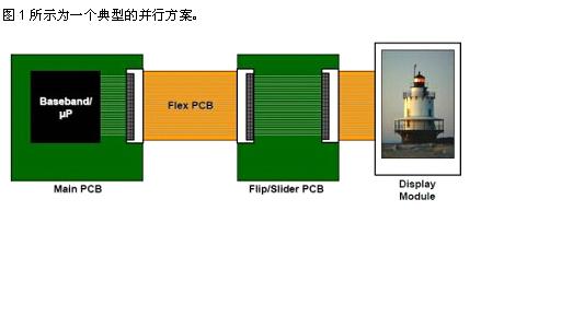
Figure 1: Typical parallel scheme.
In this architecture, the load of the baseband processor (BP) driver circuit includes the traces of the main PCB, the FPCB, the FPCB connector, and the traces on the flip PCB and the final display load. The BP driver circuit must be able to drive the load directly using LVCMOS signaling.
A display with an RGB interface may require up to 24 bits of data, and this requires a bandwidth of 8 MHz or higher for the WQVGA display, depending on the resolution of the display. The higher the resolution of the display, the greater the signal bandwidth required for the display interface.
Serial scheme:
In the serial display scheme, a pair of devices are placed on the data channels of the main PCB and the flip PCB. The serializer is located on the main PCB and converts the parallel display data into a serial data stream and transmits it to the deserializer via the FPCB. Depending on the serialization architecture used, several serial data signals can be reduced to a pair of differential signals. The deserializer converts the serial data stream into a parallel data stream that drives the display interface (see Figure 2).

Figure 2: Serial implementation.
Parallel and serial schemes have important differences, and it is these differences that enable serial schemes to reduce link power consumption. When a serializer is used on the main PCB, the requirements for the BP output driver circuit are greatly reduced because the driver load of the serializer input is much lower than that required for parallel display channels. With a serial interface, BP also reduces the output voltage and allows the serializer to handle level shifting to the display driver circuitry. For example, the display operates at 2.7V and BP reduces the output to the serializer to 1.8V. The deserializer will then generate the 2.7V signal required by the display.
In addition, most serial schemes use a differential signaling protocol similar to Low Voltage Differential Signaling (LVDS). This signal greatly reduces the voltage amplitude required to transmit data through the FPCB and also reduces EMI on the signal link. By reducing the signal amplitude and eliminating the double-shielded FPCB due to the reduced EMI in the serial stream, the serial scheme can reduce power consumption.
Power turning point:
For a given application, the transition point that starts with a serial scheme and saves power compared to a parallel scheme is the power turning point. For our example, using the empirical estimate of the system parameters, the power turning point can be approximated by comparing the display link power consumption of the serial and parallel data paths in the handset. Dynamic power can be obtained from the following equation:
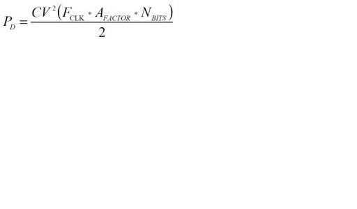
In this equation:
C = payload capacitance of the driven link
V = display voltage amplitude of the signal
FCLK = display data channel bandwidth
AFACTOR = Shows the effective activity factor of the signal (average rate of data bit level shifting)
NBITS = display channel data bit width
Figure 3: Dynamic Power Calculation
Among these parameters, most of C and AFACTOR have been discussed in this paper. C is system-dependent. For parallel schemes, C can take values ​​of 80pF to estimate PCB traces, flexible connectors, FPCB, ESD. Typical applications for /EMI components and display driver input loads. AFACTOR is related to the data and varies greatly depending on the application, but in this calculation, it is assumed to be 50%.
Using these parameters and the equation of Figure 3, the power consumption of the parallel scheme was calculated to be 29 mW according to the following parameters.
C = 80pf
V = 2.7V
Fclk = 8MHz
Afactor = 50%
Nbits = 24
For serial schemes, the power calculations are slightly different. The method used here is to simultaneously calculate the power consumption of the BP drive serializer and the power consumption of the deserializer driving the display drive circuit.
According to the following parameters, the power consumption of the BP drive serializer is 0.5mW.
C=3pf
V=1.8V
Fclk=8MHz
Afactor=50%
Nbits=24
It can be seen that due to the reduced BP output load, the voltage and drive current of the BP IO can be reduced, thereby greatly reducing power consumption.
Using the same method, the power consumption of the deserializer driving display drive circuit was calculated to be 14.5 mW according to the following parameters.
C=40pf
V=2.7V
Fclk=8MHz
Afactor=50%
Nbits=24
According to this calculation, the power turning point of this example is 14mW, which is the difference between the parallel power consumption and the parallel part power consumption of the serial scheme. This power turning point determines the threshold at which the serial link power consumption reaches equilibrium. For this example, the power consumption of the current serial scheme is below 20mW. This means that the design power consumption for increasing serialization processing is only increased by less than 6mW. If the power consumption is further reduced, such as eliminating some of the passive components commonly used in parallel schemes, the serial scheme can truly reach the power turning point.
By finely implementing serialization, the power consumption of the display data path can be further reduced, thereby increasing the power turning point, which can include eliminating some EMI components and displaying ESD protection devices on the data path because in serial schemes, serialization Theizer and deserializer pair provides ESD protection against BP and display driver circuits against current transients on the FPCB.
Another way to further reduce power consumption by the serial scheme is to integrate the deserializer into the display driver circuit, which is currently used in some applications. This greatly reduces the large capacitive load of the deserializer, further reducing power consumption. Even in applications where the deserializer is not integrated, the deserializer can be placed close to the display driver circuit, reducing the length and load of the data channel traces, which in turn reduces power consumption.
to sum up:
Serialization technology has been increasingly used in today's mobile phone designs. Serialization technology is mainly used to save space, but people often think that this will greatly increase system power consumption. This article eliminates this concern and clarifies the principle that serialization technology actually reduces power consumption. Current serialization solutions are closing the gap between serial power and power turning points. This means that in addition to the other benefits that serialization technology brings to the design, the serial solution's link power consumption can be reduced, resulting in lower overall system power consumption.
The 7-inch tablet can be used as the golden size of a tablet computer. It is small and portable. It can be used at home and outdoors. You can browse the web, watch videos and play games. It is a household artifact. Although the size of the 7-inch tablet is inclined to the tablet, the function is more inclined to the mobile phone, so it can also be used as a substitute for the mobile phone. Compared with other sized tablets, the 7-inch tablet has obvious advantages in appearance and weight. Both the body size and the body weight have reached a very reasonable amount.
1.In appearance, the 7 inch tablet computer looks like a large-screen mobile phone, or more like a separate LCD screen.
2.In terms of hardware configuration, the 7 inch tablet computer has all the hardware devices of a traditional computer, and has its own unique operating system, compatible with a variety of applications, and has a complete set of computer functions.
3.The 7 inch tablet computer is a miniaturized computer. Compared with traditional desktop computers, tablet computers are mobile and flexible. Compared with Laptops, tablets are smaller and more portable
4.The 7 inch tablet is a digital notebook with digital ink function. In daily use, you can use the tablet computer like an ordinary notebook, take notes anytime and anywhere, and leave your own notes in electronic texts and documents.
7 Inches Tablet Pc,Quad Core Tablet 7 Inch,7 Inch Gaming Tablet,Supersonic Tablet 7 Inch
Jingjiang Gisen Technology Co.,Ltd , https://www.jsgisentec.com