The RF2968 is designed for Bluetooth applications and operates in the 2.4GHz band. Complies with the Bluetooth Radio Specification version 1.1 power level two (+4dBm) or level three (0dBm) requirements. For power class 1 (+20dBm) applications, the RF2968 can be used with power amplifiers such as the RF2172. The chip contains the transmitter, receiver, VCO, clock, data bus, chip control logic and other circuits. With an integrated IF filter in the chip, the RF2968 requires minimal external components and avoids external components such as IF SAW filters and symmetrical-asymmetric converters. The high-impedance state of the receiver input and transmit output eliminates the need for an external receiver/transmitter switch. The RF2968 is connected to an antenna, RF bandpass filter, and baseband controller for a complete Bluetooth solution. In addition to RF signal processing, the RF3968 also performs baseband control, DC compensation, data and clock recovery for data modulation.
Interface Circuit Principle: The RF2968 transmitter output is internally matched to 50Ω and requires an AC coupling capacitor. The receiver's low noise amplifier input internally matches the 50Ω impedance to the front-end filter. The receiver and transmitter are connected to a coupling capacitor between TXOUT and RXIN to share a front-end filter. In addition, the transmit channel can be amplified to +20dBm by an external amplifier, and the RF2968's transmit gain control and received signal strength indication can be turned on to enable Bluetooth to operate at power level one. The RSSI data is input via the serial port and provides 1dB resolution over a power range of -20 to 80 dBm. The transmit gain control is modulated in 4dB steps and can be set via the serial port. The baseband data is sent to the transmitter via BDATA1. The BDATA1 pin is a bidirectional transfer pin that acts as an input in transmit mode and as a receive mode in transmit mode. RF2968 implements Gaussian filtering of baseband data, FSK modulated intermediate frequency current controlled crystal oscillator (ICO) and intermediate frequency IF upconversion to RF channel frequency. The on-chip voltage-controlled oscillator (VCO) produces a frequency that is half the local oscillator (LO) frequency and is then multiplied to the exact local oscillator frequency. The two external loop inductances between RESNTR+ and RESNTR- set the VCO's regulation range. The voltage is fed from the on-chip regulator to the VCO, and the regulator is connected in the middle of the two loop inductors via a filter network. Loop filters (connected to DO and RSHUNT) are especially important due to the need for Bluetooth fast frequency hopping, which determines the VCO transition and setup time. Therefore, it is highly recommended to use the component values ​​provided in the circuit diagram. The RF2968 can use a reference clock frequency of 10MHz, 11MHz, 12MHz, 13MHz or 20MHz and can support 2 times the reference clock of these frequencies. The clock can be sent directly to the OSC1 pin by an external reference clock through a DC blocking capacitor. If there is no external reference clock, the crystal oscillator and two capacitors can be used to form the reference oscillator circuit. Whether it is an external or internally generated reference frequency, use a resistor connected between OSC1 and OSC2 to provide the proper bias. The frequency tolerance of the reference frequency shall be 20 & TImes; 10-6 or better to ensure that the maximum allowable system frequency deviation remains within the demodulation bandwidth of RF2968. The LPO pin provides a low frequency clock to the baseband device in sleep mode with a 3.2 kHz or 32 kHz low power mode clock. Taking into account the minimum sleep mode power consumption and flexible selection of the reference clock frequency, a 12MHz reference clock can be selected.
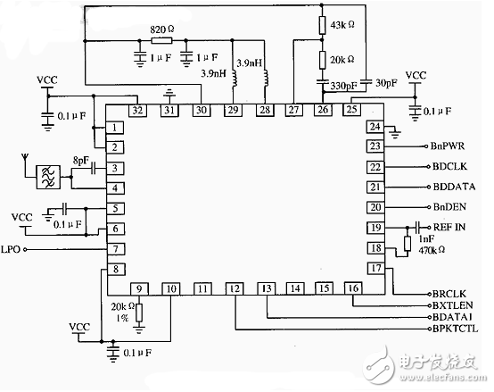
The receiver uses a low IF structure to minimize external components. The RF signal is downconverted to 1 MHz, allowing the IF filter to be implanted into the chip. The demodulated data is output on the BDATA1 pin, and further data processing is done with baseband PLL data and clock recovery capacitors. D1 is the connection pin of the baseband PLL loop filter. The sync data and clock are output on the REDATA and RECCLK pins. If the baseband device uses RF2968 for clock recovery, the D1 loop filter can be omitted.
8GPU 847-Pro Mining Rig(Black)
We offer a wide variety of cypto mining products as you need.
Large Port Gap Between GPU: The GPU interface spacing is 65mm, and the space is larger than other miners. Therefore, it will have better heat dissipation performance, which can ensure low power consumption, less heat generation, energy-saving, and safe use.
8 GPU Ports: The Motherboard of the mining machine comes with 8 GPU interfaces, and 8 GPUs can be installed at the same time. With 8 GPUs working at the same time, the performance of the BTC/ETH/ETC mining machine system will be greatly improved. The actual work done for you is lasting and rewarding.4 Cooling Fans: The pre-installed large-flow cooling fan of the mining machine chassis can accelerate air convection, strengthen heat dissipation, ensure good heat dissipation, and extend the life of the graphics card.
CPU Radiating: A good heat dissipation effect to prevent the motherboard from overheating during work, the actual work done for you is lasting and rewarding.
Applicable graphics card: GPU P104,GPU P106,GPU 1660,GPU 3060,GPU 3070,GPU 3080,GPU 580,GPU 598, GPU 5600XT,GPU 5700XT
ethereum mining rig,ethereum mining,eth mining,buy ethereum miner,ethereum gpu mining
Easy Electronic Technology Co.,Ltd , https://www.pcelectronicgroup.com