Circuit function and advantage
The circuit shown in Figure 1 is a complete, unregulated linear variable differential transformer (LVDT) signal conditioning circuit. This circuit accurately measures linear displacement (position).
The LVDT is a highly reliable sensor because its core can slide without friction and has no contact with the inside of the tube. Therefore, LVDT is suitable for use in flight control feedback systems, position feedback in servo systems, automatic measurement in machine tools, and a variety of other industrial and scientific electromechanical applications that focus on long-term stability.
This circuit uses the AD698LVDT signal conditioner, which includes a sine wave oscillator and a power amplifier to generate the excitation signal that drives the primary LVDT. The AD698 also converts the secondary output to a DC voltage. The AD8615 rail-to-rail amplifier buffers the output of the AD698 and drives a low-power, 12-bit successive approximation analog-to-digital converter (ADC). With a system dynamic range of 82 dB and a bandwidth of 250 Hz, it is ideal for precision industrial location and metrology applications.
With a ±15 V supply, the system's signal conditioning circuitry consumes only 15 mA; with a +5 V supply, it consumes 3 mA.
This circuit note discusses the basic operating theory and design steps of the LVDT to optimize the bandwidth given circuit in Figure 1, including noise analysis and device selection considerations.
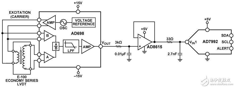
Figure 1. General LVDT Signal Conditioning Circuit (Simplified Schematic: All Connections and Decoupling Not Shown)
Circuit description
working principle
The LVDT is an absolute displacement sensor that converts a linear displacement or position from a mechanical reference point (or zero point) to a proportional electrical signal containing phase (direction) and amplitude (distance) information. LVDT operation is accomplished without the need for electrical contact between the moving parts (probe or core rod assembly) and the transformer. It relies on electromagnetic coupling. For this reason, plus it does not work with built-in electronic circuitry, LVDT is widely used in applications requiring long life and high reliability in certain environments, such as military and aerospace applications.
For this circuit, the E-100 economical LVDT sensor series from Measurement SpecialTIesTM, Inc. is used with the AD698. The E-Series has a linearity of ±0.5% over the entire range and is suitable for most applications in moderate operating temperature environments.
The AD698 is a complete LVDT signal conditioning subsystem. It converts the mechanical position of the LVDT sensor to a unipolar DC voltage with high accuracy and repeatability. All circuit functions are integrated on-chip. By adding several external passive components to set the frequency and gain, the AD698 converts the raw LVDT secondary output to a proportional DC signal.
The AD698 contains a low-loss sine wave oscillator that drives the primary side of the LVDT. The sine wave frequency is determined by a single capacitor with a frequency range of 20 Hz to 20 kHz and an amplitude range of 2 V RMS to 24 V RMS.
The LVDT secondary output consists of two sine waves that drive the AD698 directly. The AD698 decodes the LVDT by synchronously demodulating the amplitude modulation input (secondary, A) and the fixed input reference voltage (primary, secondary, or fixed input, B). A common problem with previous solutions is that any drift in the amplitude of the drive oscillator directly results in a gain error in the output. The AD698 calculates the ratio of the LVDT output to its input excitation, counteracting the effects of any drift, thereby eliminating these errors. Unlike the AD598 LVDT signal conditioner, the device has different circuit transfer functions and does not require the LVDT secondary-side summation (A + B) to be consistent with the stroke length.
The block diagram of the AD698 is shown in Figure 2. The input consists of two independent synchronous demodulation channels. The B channel monitors the drive excitation of the LVDT. C2 filters the full-wave rectified output and sends it to the arithmetic circuit. Channel A performance is identical except for the externally supplied comparator pins. Since the A channel may reach the 0 V output when the LVDT is empty, the demodulator of the A channel is typically triggered using the primary side voltage (B channel). In addition, a phase compensation network may be required to add phase lead or lag to the A channel to compensate for the phase shift from the primary to secondary side of the LVDT. For a half-bridge circuit, the phase shift is not critical and the A-channel voltage is sufficient to trigger the demodulator.
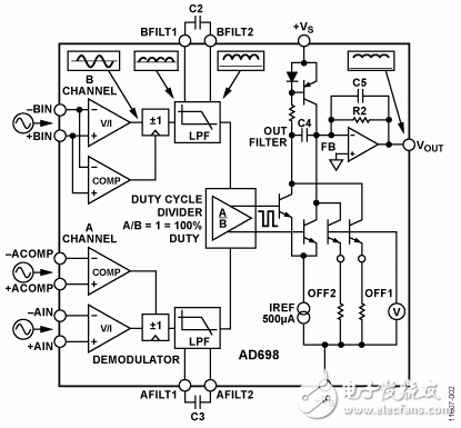
Figure 2. Block diagram of AD698
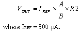
After both channels have been demodulated and filtered, a voltage divider circuit equipped with a duty cycle multiplier is used to calculate the A/B ratio. The output of the voltage divider is the duty cycle. If A/B is equal to 1, the duty cycle is 100%. (This signal can be used if a pulse width modulated output is required). A duty cycle drive circuit that modulates and filters a reference current that is proportional to the duty cycle. The output amplifier regulates the 500 μA reference current and converts it to voltage. The output transfer function is:
Nanning Ousibang Information Technology Co., Ltd. , https://www.ousibangvape.com