Most of the FPGA devices are based on the RAM structure. Of course, there are also Flash-based structures, but the RAM structure is the mainstream, which is also the focus of our discussion. RAM is a volatile memory, and the data stored on it after power-off is lost. After re-powering, the configuration data needs to be loaded again. Therefore, we certainly don't want to use a PC to load once every time we re-power it, and engineering applications don't allow us to do this. Therefore, there is a configuration chip next to the FPGA, which is usually a flash memory. Whether it is serial or parallel Flash, their startup loading principle is basically the same.
To avoid confusion, here is a little distinction between the FPGA download configuration and the boot configuration. The download configuration of the FPGA device refers to burning the FPGA configuration data stream on the PC into the FPGA or Flash memory through the download cable. The startup configuration of the FPGA device refers to loading the configuration data stream from the PC or Flash memory into the FPGA to make it run.
The download configuration of the FPGA device, the most common is based on the JTAG configuration mode, which can directly load the configuration data stream on the PC to the FPGA for online operation, or indirectly burn the data to the Flash through the FPGA device itself. Wait for external configuration chips. Another download configuration is to download the configuration data stream directly to the configuration chip. Because the JTAG method is flexible and versatile, especially online debugging is very fast and convenient, only the JTAG interface is reserved in our FPGA core board circuit.
The startup configuration of the FPGA device mainly includes JTAG mode, AS and PS configuration mode.
The AS configuration mode is guided by the FPGA device configuration process, which controls the external memory and its initialization process. The FPGA device is in an active position and the configuration device is subordinate. Configuration data is fed into the FPGA through the DATA0 pin. The configuration data is synchronized on the DCLK input and transmits 1 bit of data in 1 clock cycle.
The PS configuration mode is controlled by the PC or other controllers. During PS configuration, configuration data is sent from the external storage device to the FPGA through the DATA0 pin. The configuration data is latched on the rising edge of DCLK and transmits 1 bit of data in 1 clock cycle.
The JTAG interface is an industry standard for chip testing and other functions. It uses the IEEE Std 1149.1 joint boundary scan interface pin and supports the JAM STAPL standard, which can be done using the Altera download cable or the main controller.
When the FPGA is in normal operation, its configuration data is stored in RAM and must be re-downloaded when power is applied. In the experimental system, the computer or controller is usually used for debugging, so the PS configuration method can be used. In a practical system, in most cases, the FPGA must actively boot the configuration operation process. At this time, the FPGA will actively obtain the configuration data from the peripheral dedicated memory chip, and the FPGA configuration information in this chip is the pof format designed by the ordinary programmer. The file was burned in.
The principle of downloading FPGA in JTAG mode is shown in Figure 2.21. The Quartus II software on the PC downloads the configuration data stream (sof file) to the FPGA through the download cable. After the download is completed, the FPGA immediately executes the download code, which is very fast. Suitable for debugging.
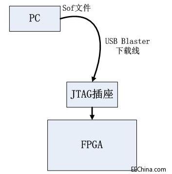
Figure 2.21 JTAG mode download configuration process
The principle of FPGA downloading data to the configuration chip is shown in Figure 2.22. The Quartus II software on the PC side downloads the configuration data stream (jic file) to the configuration chip through the download cable. Since the configuration chip and the JTAG interface are respectively connected to the FPGA, they are not directly connected, so the configuration file is transferred from the PC to the FPGA first, and then the FPGA is internally transferred to the configuration chip. In this process, the FPGA functions as a bridge.
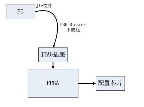
Figure 2.22 JTAG mode to download data to the configuration chip
After reading the principle of configuring the FPGA and programming the chip in JTAG mode, let's take a look at the initial configuration process of the FPGA power-on. After the FPGA is powered on, the internal controller first works to confirm the current configuration mode. If the external configuration chip is started, the data of the configuration chip is loaded into the RAM of the FPGA through the interface with the external configuration chip (such as our SPI interface). In the middle of the configuration, the official operation begins. Of course, some people may wonder if the JTAG online configuration conflicts with the configuration chip loading. No, the JTAG online configuration has the highest priority. No matter what logic is running in the FPGA at this time, as long as the JTAG download is started, the FPGA stops the current work and starts running the new configuration data of the JTAG download.
Let's look at some of the related reference designs given in the device manual, as shown in Figure 2.23. This is the interface between the FPGA and the SPI Flash used for configuration, which is what we call the AS configuration. Note that the connection of several main pins of the FPGA, nSTATUS\CONF_DONE CONFIG CE, or pull-up, or grounding, is mainly to ensure that these signals are initially in a certain level state during power-on, preventing false levels from causing false triggers. The four pins DATA\DCLK\NCSO\ASDO are the SPI interface and are connected to the SPI Flash.

Figure 2.23 Screenshot of the AS configuration reference circuit
As shown in Figure 2.24, the FPGA has a group MSEL pin that is used to set the startup mode when the FPGA is initially powered up. Our FPGA power-up uses the Standard AS mode to load configuration data from the SPI Flash.

Figure 2.24 Screenshot of the MSEL pin configuration description
With the previous theory to pave the way, our design is based on evidence. As shown in Figure 2.25, this is our SPI FLASH chip, which has four signals connected to the corresponding pins of the FPGA device.
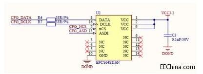
Figure 2.25 FPGA AS Configuration Circuit
The front is the circuit that powers up the configuration data, which is implemented by an SPI Flash. The PC-to-FPGA device download is implemented by JTAG. The JTAG concept network is flying all over the world. Everyone has to digest it. However, wherever there is a CPU, there is basically JTAG, and FPGA is no exception. In addition, everyone noticed that the previous MSEL set the FPGA boot mode to Standard AS mode, but JTAG is always the highest priority mode. At any time, as long as JTAG needs to be downloaded and configured, the configuration mode will be converted. The connection circuit of the JTAG download socket and some configuration dedicated pins is shown in Figure 2.26.
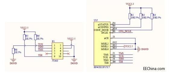
Figure 2.26 JTAG socket and FPGA configuration circuit
Longkou Libo Insulating Material Co.,Ltd. , https://www.liboinsulation.com