Today, most electronic instruments use embedded systems. Typically these embedded systems include sensors, amplifiers for buffering and conditioning signals, analog-to-digital converters, and microcontrollers for data processing and human-machine interfaces. For example, data acquisition systems and data loggers are such systems. Figure 1 shows a block diagram of a data acquisition system with a USB interface.
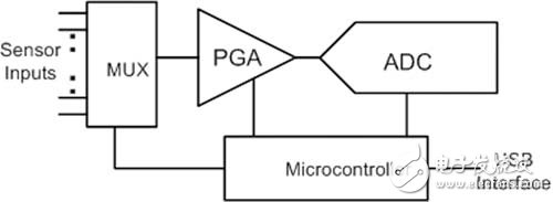
Figure 1 Data acquisition system with USB interface
The sensor on the output has a range of features. Among them, the sensitivity and dynamic range of the sensor are most important for scaling the sensor's signal to the input range of the analog-to-digital converter (ADC). Multiplying the sensitivity of the sensor by the maximum value of the measured mass is equal to the maximum output of the sensor. In many cases, the sensor's output must be amplified to take full advantage of the ADC's input range. Figure 2 shows the relationship between the two.
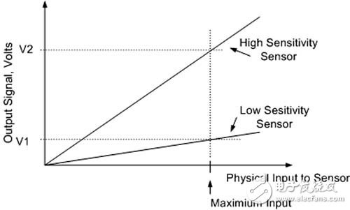
Figure 2 Sensor output as a function of sensitivity
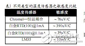
Three different types of temperature sensors are now compared, which are thermocouples, RTDs (resistance temperature detectors) and LM35 wafer temperature sensors.
Referring again to Figure 1, it can be seen that the role of the PGA (Programmable Gain Amplifier) ​​is to scale the sensor's signal to the input range of the ADC. The gain function of the PGA is preferably digitally controlled by a microcontroller due to the application trend of today's USB, IP and other communication links. Although there are several different PGA options available today, users tend to use binary amplification methods such as 1, 2, 4, 8, 16... or other magnifications. For this type of data acquisition system, the ideal amplifier should be divided into several small and uniform gain levels over the entire gain range. In addition, flexible system calibration and other adjustments can be provided to the instrument by integrating the system, software-controlled functions, and the ability to configure system gain and signal path characteristics during operation.
National Semiconductor's recently introduced LMP8100 programmable amplifiers feature new digital programmability. By using standard interface communication protocols, SPI bus, gain, frequency compensation, zero input, and power saving can be implemented at low cost and high efficiency. These signal path functions are controlled by software and add value to the design of sensor interfaces, offset correction and broadband control.
The following sections discuss the implementation of a PGA with unity gain in a USB link data acquisition system.
Features of the LMP8100
The LMP8100 implements four programmable functions:
1. Non-inverting-gain can be selected step by step from gain 1 to 16.
2. Internal frequency compensation can be programmed to one of four values.
3. The input to the amplifier can be disconnected from the input signal and connected to ground. The offset voltage of the amplifier can be measured.
4. The amplifier can be programmed to power save mode to minimize power consumption.
Figure 3 shows a simplified schematic of an LMP8100.
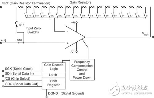
Figure 3 Schematic of the LMP8100
The function of the LMP8100 is programmed with an 8-bit binary value and is shifted into a serial data input pin. Table 2 shows the bit allocation of the control registers.
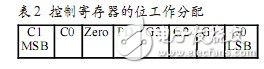
Table 3 shows the assignment of gain, zero, and power-saving logic levels.
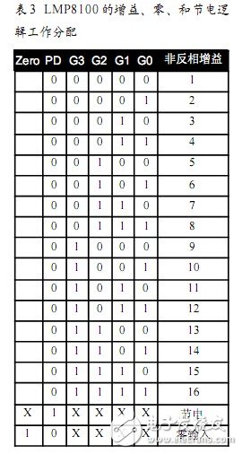
Table 4 shows the logic level work assignment for frequency compensation.

Minimum compensation
The control register is programmed by shifting eight bits of data into the serial data input pin at the clock timing on the serial clock pin. Figure 4 is a timing diagram of shifting data into a control register. It can be seen that the double buffering and loading of the control register can be divided into two steps. The first step is to shift the data into the shift register using eight clock cycles. The data in the shift register is then transferred in parallel to the holding registers at the rising edge of the chip select signal, while the output of the holding registers is used to select functions such as gain, frequency compensation, power saving, and zero input. This method prevents the state of the amplifier from changing until the data is correctly shifted into the shift register.
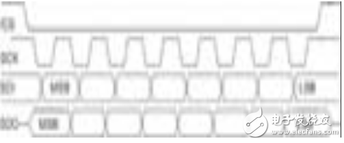
Figure 4 LMP8100 serial data transfer
Previously generated data will be used to design a programmable gain amplifier for use in a USB data acquisition system. If you have decided to use a 12-bit ADC with a 4.096V reference with a resolution of 1mV, how much gain is needed to amplify the output of an ordinary sensor to this value? At this point, a simple review of the sensor's sensitivity and the measured variable span reveals that the full-scale output range of a given sensor can range from 2mV to 3V. This means that the highest gain is about 205. The following equation EQ1 shows the relevant calculation.
Maximum gain = full input / maximum sensor output = 4.096V / 0.020V = 204.8 (1)
This maximum gain range from 1 to 205 can be achieved by connecting two LMP8100s in series. Connecting the gains of the two amplifier stages together increases the amplitude, allowing the programmable gain range to be extended from 1 to 256. Figure 5 is an implementation of the two LMP8100s connected in series. Each amplifier can program the gain from 1 to 16, so the total gain range is 1 to 256 and is measured in increments per unit.
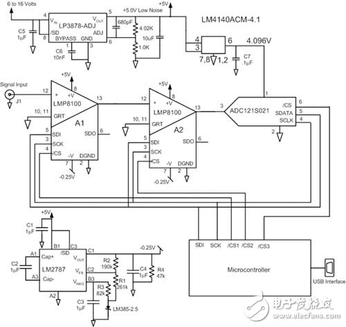
Figure 5 Programmable Amplifier for Data Acquisition Systems
In addition to the programmable gain, other functions of the amplifier can be controlled by the program. In most data acquisition and recording applications, measurements are typically performed at regular intervals. For example, every two seconds or every 10 seconds, etc. In these applications, the amplifiers can enter a power-saving state, and the power consumption of each amplifier is reduced to 40μA. This feature reduces battery life by reducing the average supply current consumption in portable systems.
The function of the zero function is to correct the offset voltage in the amplifier by software. The software program sets a gain for the expected measurement and sets a zero width in amplifier A1. In this configuration, the output voltage of amplifier A2 is the offset voltage for the intended measurement, and this value is stored by the software and is reserved for the next step. Then, the zero in A1 will be cleared, and the measurement will be performed at this time, and the offset voltage value will be subtracted from the measured value of the signal. In this way, the offset voltage and offset voltage drift at any given gain setting can be compensated.
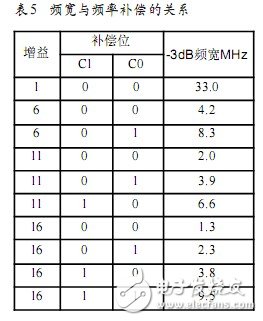
The LMP8100's programmable frequency compensation expands the bandwidth at high gain when needed. Table 5 shows the amplifier bandwidth at several different gain settings for the setting of the frequency compensation bits. As can be seen from the figure, setting a compensation bit in the control register reduces the internal frequency compensation of the amplifier. At low gains, there is a possibility that the amplifier and ringing compensation are insufficient, and even oscillation may occur.
Referring to Figure 5, a 0.25V negative supply voltage function was added to the design. This feature corrects two problems with single-supply design while maintaining the voltage on the amplifier below the maximum operating voltage of 5.5V:
1. Considering that the input to A2 is zero volts, the typical output swing of the LMP8100 is as low as 50mV, but can be as high as 150mV. In this case, if a 12-bit ADC is assumed to have a voltage reference of 4.096V, the code of the ADC from 50 to 150mV is not available.
2. Considering that the input to A1 is zero volts, the lowest output voltage of 50 to 150 mV is multiplied by the gain setting of A1. In this case, the minimum output voltage of A2 can be as high as 2.4V (0.150 x 16). Similarly, assuming a voltage reference of 4.096V, this means that 59% of the input range of the ADC is not available.
The LM2787 is a switched capacitor inverter with a low noise adjustable linear regulator. A negative supply voltage of 0.25V is generated by using a negative 2.5V voltage reference plus the feedback resistors R1 and R2 and the internal voltage reference of the LM2787. By supplying a small negative voltage to the LMP8100, the zero-volt output swing problem is solved, as well as the two problems mentioned above.
In summary, the programmable gain amplifiers discussed in this paper are designed with superior gain control for a wide range of sensor interface applications.
Energy-saving Hospital Elevator
Bed Frame Elevators,Energy-Saving Elevator,Energy Efficient Elevators,Energy-Saving Hospital Elevator
XI'AN TYPICAL ELEVATOR CO., LTD , https://www.chinaxiantypical.com