For complex systems, robustness is very important. To assist customers in building robust systems, KeyStone devices offer a variety of hardware protection mechanisms such as memory protection and EDC. This article describes how to use these features to build a robust system on KeyStone devices. Routines accompanying the documentation are also provided.
1 Introduction
As shown in Figure 1, KeyStone devices offer a variety of features that help customers build robust applications.
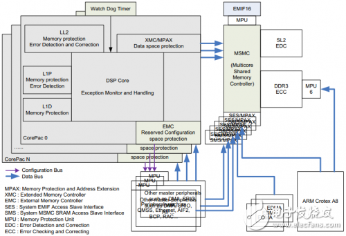
Figure 1 KeyStone device robust system
As shown in Figure 1, the memory protection module is integrated in LL2, L1P and L1D; the error checking correction module is integrated in LL2, SL2 and DDR controllers; L1P integrates error detection module. MPAX and MPU modules are attached to the bus for monitoring and detection to avoid illegal bus access. Each DSP CorePac has a separate MPAX for monitoring the bus connected to the MSMC.
For other masters in the system, they are classified according to the permission ID. For each privilege ID, two MPAXs are integrated in the MSMC to monitor access related to the privilege ID. One is SES MPAX to protect access to DDR3 and the other is SMS MPAX to protect access to SL2. For the authority ID corresponding to each master, refer to the corresponding device manual.
An MPU has been added to the configuration ports of some peripherals to protect against unauthorized access to the peripheral's configuration area. However, not all peripherals are protected by the MPU. Refer to the list of peripherals protected by the MPU in the corresponding device manual. Each CorePac has a watchdog timer that monitors its activity. If the core dies, the watchdog can trigger a non-maskable interrupt or reset signal.
EMC can avoid the DSP core from accessing unmapped configuration space, and XMC can avoid DSP core access to unmapped data space. All of these features are implemented by hardware modules, and using these features has essentially no effect on system performance. Using EDC has a slight impact on memory access performance, but it is almost trivial from the overall system level.
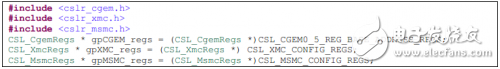
In the event of a problem, all of these modules can trigger an exception to the DSP core, and the DSP core's exception monitoring module can log these states and trigger the exception service routine to perform the appropriate action. This article discusses the application of these features and gives examples of related register-based CSL implementations. The code defines the register pointer as follows.
The above various characteristics are described in detail in the documentation of the respective subsystems, and all relevant documents are listed in the reference chapter at the end of this article. Before looking at this article, it is assumed that the customer has read the documentation corresponding to the relevant attributes, so this article aims to provide relevant supplementary information.
This article applies to the KeyStone 1 Series DSP, and the routines are validated on the TCI6614 EVM, C6670 EVM, and C6678 EVM. For other KeyStone devices, the KeyStone 2 series is the same. The basic functions are the same. For some differences in details, please refer to the corresponding device manual.
2 memory protection
The memory protection properties on KeyStone devices are discussed in the document "Memory ProtecTIon On KeyStone Devices (SPRWIKI9012)", which includes many useful information not found in other documents. This section summarizes and supplements them.
Table 1 summarizes the differences between the different memory protection modules.
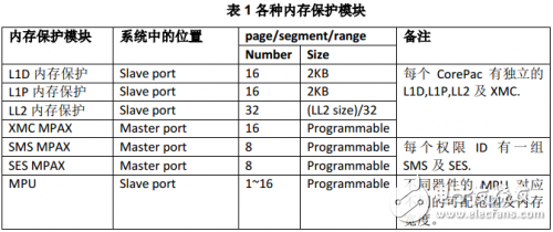
There are multiple masters and slaves in the system. The protection module on the slave input port is used to block illegal access from the other masters to the slave. The protection module on the master output port is used to prevent the master from illegally accessing all other slaves. The protection properties of each memory page, slice or range are programmable.
2.1 L1 and LL2 memory protection
For basic information about L1 and LL2 memory protection, refer to the Memory Protection section of the TMS320C66x CorePac User Guide (SPUGW0).
L1 and LL2 memory protection only distinguishes between 7 external request IDs, but the system may have 16 permission IDs. By default, system privilege IDs 0~5 are mapped to CorePac AID 0~5, and all other privilege IDs are mapped to AIDx.
The mapping between CorePac AID and system privilege ID can be configured by EMC programming. Refer to the “External Storage Controller (EMC)†section of the “TMS320C66x CorePac User Guide (SPUGW0)†for details. Note that the AID of the IDMA is the same as the value of the CorePac to which it belongs. The ID of the EDMA transmission is the same as the number of the core that configured and initiated the transmission.
Usually L1 is configured as a cache, in which case all L1 related memory protection attribute registers should be cleared to prevent other masters from accessing L1.
The registers of the CorePac internal memory protection module (protecting L1, LL2 and XMC/MPAX) are protected by a lock. By default, these registers are not locked, and the user software can lock these registers with a custom key, which can then be accessed only after unlocking with that key.
2.2 Shared Memory Protection – MPAX
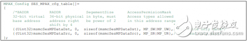
For basic information about CorePac shared memory protection, refer to the "Extended Storage Controller (XMC)" section of the "TMS320C66x CorePac User Guide (SPRUGW0)". For basic information about shared memory protection of other masters in the system, refer to "KeyStone Architecture MulTIcore Shared Memory Controller User". "Memory Protection and Address Extension (MPAX)" chapter in Guide (SPRUGW7). The following is a sample configuration of the XMC/MPAX in the routine, each line representing a slice configuration in the MPAX.
Address access with a logical address below 0x0C00_0000 does not enter the XMC. For address space 0x0000_0000~0x07FF_FFFF
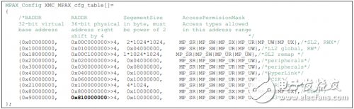
Address resolution is performed inside the C66x CorePac when accessing. This address range includes internal and external configuration buses, as well as L1D, L1P, and L2 memory. When accessing the logical address located in the interval 0x0C00_0000~0x0FFF_FFFF, the L1 cache is passed, and the prefetch cache is performed during the read operation. The memory attribute configuration register MAR corresponding to the address range is hardware-stretched and cannot be modified. That is to say, the access to the logical address space does not pass through the L2 cache before entering the XMC MPAX, so this logical address space is called the "fast SL2 RAM path". For logical address accesses greater than or equal to 0x1000_0000, the first pass through the L2 cache controller and then through the XMC MPAX will increase the latency of one cycle.
According to the above configuration example, when accessing SL2, the access rate using the logical address 0x0C00_0000 is higher than the logical address 0x1800_0000 after the remapping is used. However, the memory attribute register MAR corresponding to 0x1800_0000 is programmable, so SL2 accessed through 0x1800_0000 can be configured as non-cacheable and non-prefetchable.
Note that the replacement address RADDR is a 36-bit physical address >>4. Common DDR3 error configurations are as follows:
![]()
or

Note that the DDR3 starting physical address is 0x8:0000_0000, and 0x9:0000_0000 has a 4GB offset from the starting address, which is an illegal address in most systems.
In a real system, you should make full use of all the fragments of MPAX to better divide the storage space into as many small pieces as possible, and carefully set the access qualification properties of each fragment.
Unused addresses should not be mapped, and MPAX will refuse to access unmapped addresses and report exception events, helping to catch software errors.
SMS/MPAX only allows access to SL2, as follows for its configuration example:

SES/MPAX is used to protect access to DDR3, as follows for its configuration example:
When two masters exchange data through shared memory, you should ensure that the logical addresses used by the two masters are mapped to the same physical address. Note that the EDMA's permission ID is inherited from the CorePac configured for it.
caveat:
When modifying an MPAX entry, you need to ensure that there is no access to the address covered by the entry. Before the modification, the data in the cache corresponding to the address coverage address and the prefetch cache needs to be written back and invalidated.
For MPAX configuration, it is recommended to complete the program at the beginning of the program and before using any shared storage space. The code and data for the CorePac MPAX configuration should be placed in LL2.
If you want to dynamically modify an MPAX entry at runtime, the safe way is to write the new configuration to an unused numbered height table entry and then clear the old one. This is because the numbered height table entry has a higher priority than the numbered low-end entry.
Before modifying an MPAX entry, you need to perform the following operations:
1. The storage space content corresponding to the MPAX entry is removed from the cache. Even for storage spaces where the attribute is not writable, CACHE_wbInvL2() should be used instead of CACHE_inv L2().
2. If the prefetch function is enabled for the affected memory space, then the invalidation operation needs to be performed on the prefetch cache.
3. Execute "MFENCE" to ensure that the write back and invalidation operations are completed.
The CorePac's MPAX registers are protected by CorePac's memory protection register locks. The MPAX memory protection attribute registers of SES and SMS are used internally by the MSMC for SES and SMS lock protection. Other registers within the MSMC are internally protected by the MSMC for non-MPAX locks.
2.3 Peripheral Configuration Port Protection – MPU
For basic information about the MPU, refer to "KeyStone Architecture Memory ProtecTIon Unit User Guide (SPRUGW5)".
MPU0, MPU1, MPU2, and MPU3 are identical for all KeyStone 1 devices. However, for different devices, the number of additional MPUs, the number of address range entries supported by each MPU, and the default configuration of the MPU are different. Refer to the “Memory Protection Unit (MPU)†section of the relevant device manual for details.
The difference between the MPU and the MPAX is that if the access address is not within any of the MPU address ranges, the address access is allowed; and when the address does not match the address range of any entry in the MPAX, the address access is denied.
Note that if not rejected by the MPPA settings, all access to the MPU unit by default is permitted. For an address access, the MPU first checks the access ID ID with the AID bit configuration of the MPPA register. If the AID bit corresponding to the privilege ID is 0, the address range does not need to be checked, and the access is permitted. If MPPA=0, all access to the space is allowed. If you want to deny any access to the space, you need to configure MPPA to 0x03FFFC00. The MPPA settings for L1 and LL2 memory protection are different. When the AID bit in MPPA is 0, the corresponding access is denied.
When a transmission matches multiple address ranges in the MPU, all overlapping ranges must be allowed access, otherwise the access will be denied. The final access granted is the same as the lowest of all matching entries. If a transmission matches two entries, one of which is RW and the other is RX, the final permission is R. This is not the same as MPAX. If an address falls into multiple MPAX entries, the entry with the higher number takes precedence over the entry with the lower number. MPAX will only use the highest numbered entry to determine permissions and ignore other matching entries.
The following is an example of the configuration of the MPU1 in the corresponding routine of this article. Each row represents a configuration range in the MPU.

As explained above, the queue protection is as follows:
Queues 0~2047 can only be written by AID0~7 (PUSH);
Queues 2048~6143 can be written (PUSH) by all AIDs other than AID11;
Queues 6144~8191 can only be written (PUSH) by AID8~15 (except AID11).
The MPU6 on the TCI6614 is used to avoid ARM's illegal operation of DDR3. Note that MPU6 is a protection for low 32-bit DDR physical address ranges. Note that in order to clear the MPU exception/interrupt event, a 0 must be written to the EOI register at the end of the service routine.
The TCI6614's MPU event is different from other KeyStone devices. All MPU0~7 events in the TCI6614 are combined into one event and connected to CIC0 as a system event. Since the TCI6614 MPU event is a level interrupt rather than a pulse interrupt event, all MPU event flags must be cleared before the CIC flag can be cleared. For pulse interrupt events, the CIC flag must be cleared and then cleared.
In addition, the MPU 5 for BCP in the TCI6614 can be accessed only after the BCP is enabled through the PSC. That is, when accessing the MPU5 register in the TCI6614, if the BCP is not enabled at this time, the access will trigger an access error.
2.4 Reserved area protection
The reserved area (illegal address) is automatically protected. When a read operation is performed on an illegal address, garbage data is returned and the write operation is blocked. Access to the reserved area can generate exceptions, which is good for capturing software bugs.
Since the access of the DSP core passes through the L1D controller, the access of the DSP core to the illegal address triggers the L1D memory protection exception. When the DSP core executes from an illegal address, it will trigger an instruction to get an exception. For an illegal write operation, the exception that is triggered depends on the corresponding destination address. When the DMA accesses an illegal address, the DMA module reports a bus error. A DMA error event can be routed as an exception to the DSP core.
3 EDC
EDC (Error DetecTIon and Correction) is used for Memory Soft Error. A soft error is a wrong signal or data, but it does not mean that the hardware is corrupted. After observing a soft error, it does not mean that system reliability will drop. This type of error in a spaceship is called a single event disturbance. In a memory system, a soft error changes an instruction or a data value in the program. Soft errors can usually be corrected by a device reboot, and hardware errors are usually not restored by a reboot. Soft errors do not cause damage to the system hardware; they only cause errors in the code or data being processed. The reasons for soft errors are:
1. Alpha particle radiation and cosmic rays produce energy neutrons and protons. The probability of occurrence depends on the geographical location of the device and its surroundings. Usually, a device will appear several times in a few years.
2. Soft errors can also be caused by random noise, interference, or signal integrity errors, such as on-board electrical or capacitive crosstalk. If the soft error transmission probability is higher than the theoretical value in item 1 above, you should check the hardware design to find out other reasons. A common cause is that the power supply voltage is lower than expected, causing the device to be more sensitive to the effects of noise or interference.
The EDC mechanism is implemented in all levels of KeyStone devices. The following table compares the implementation mechanisms of different memory modules.
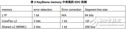
3.1 L1P error detection
For basic information about L1P and LL2 EDC, refer to the "TMS320C66x DSP CorePac User Guide (SPRUGW0)". Check Bit Generation and Check: Check bits are generated when a 64-bit aligned DMA write or L1P cache is being buffered. Non-64-bit aligned DMA access will invalidate the verification information. The L1P EDC logic checks the parity information during a 256-bit aligned program read or a 64-bit aligned DMA read.
Error check settings: The L1P error check feature is turned off by default after a device reset. Once the "EN" bit in the L1PEDCMD register is set, the ED logic in all L1P memories is enabled. The following is an example of the L1P ED function enablement extracted from the application code.
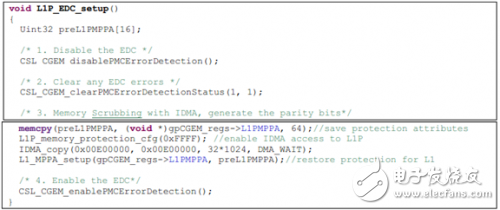
Note: For the L1P ED function to work properly, the L2 EDC must be enabled at the same time.
Error handling when accessing L1P cache: There is no dedicated system event for the validation error generated by the program acquired from the L1P cache. However, the error detection logic will send a direct exception event to the DSP (IERR.IFX event), then Users can get this error using an internal exception event. The PERR bit of the L1PEDSTAT register will be set. The L1PEDARRD register records the address information containing the error bit. In the exception handling service function corresponding to the L1P error, the cache line containing the wrong address needs to be invalidated.
Error handling for DMA access: A verification error for DMA/IDMA access, corresponding to #113 system event. Users can use this event to get the error. The DERR bit of the L1PEDSTAT register is set and the L1PEDARRD register records the address information containing the error bit.
L1P EDC Functional Verification: The L1P EDC logic can be suspended by asserting the SUSP bit in the LPEDCMD register. Using this feature, software can emulate EDC errors and verify EDC functionality. The code for verifying the L1P EDC function is provided in the routine corresponding to this article, corresponding to the function L1P_ED_test().
3.2 LL2 error checking and correction
Check bit generation and verification: Corresponding verification information is generated when a memory write operation is performed on L2 in units of 128 bits. A write operation that is not 128-bit aligned or less than 128 bits will invalidate the checksum information. The LL2 EDC logic checks the parity information for a 128-bit aligned memory read operation. Refer to the "TMS320C66x DSP CorePac User Guide (SPRUGW0)" for more information.
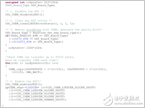
Error checking and correcting configuration: By default, the LL2 EDC feature is turned off after a device reset. Unlike some C64+DSPs, KeyStone DSP cannot enable EDC for memory partitioning. Once EDC is enabled, the EDC logic is valid for the entire CorePac L2 memory. However, different memory access requesters can be enabled separately, such as an L1D controller, an L1P controller, or a DMA controller. For example, if the user only needs to use EDC for the code segment, the following three fields need to be enabled:
1. Set the EN bit in the L2EDCMD register to enable the LL2 EDC logic;
2. Set the PL2SEN bit in the L2EDCEN register to enable the L1S memory's EDC logic to check for L1P access;
3. Set the PL2CEN bit in the L2EDCEN register to enable the L2 cache's EDC logic to check for L1P access.
The LL2 EDC logic does not initialize the verify RAM from the shutdown to the enable state transition. Therefore, after entering the enable state, the value in the verify RAM is a random value that needs to be initialized by the user software. The configuration of the L2 EDC must follow the EDC configuration sequence set forth in the "TMS320C66x DSP CorePac User Guide (SPRUGW0)". The following is an L2 EDC enable function reference code extracted from the routine:

Access error handling from the L1D controller: When data is fetched from LL2 via the L1D cache, all of this data is checked for errors, but there is no correction. Regardless of whether it is a 1-bit or multi-bit error, it will be reported to the DSP core via the #117 system event (L2_ED2: Uncorrectable Bit Error Detection).
Access error handling from L1P and DMA controllers: 1-bit errors can be corrected and reported via #116 system event (L2_ED1: bit error that can be corrected). A 2-bit error can be detected and reported via the #117 system event. The following table lists the corresponding 1-bit error handling details for different memory access requesters.
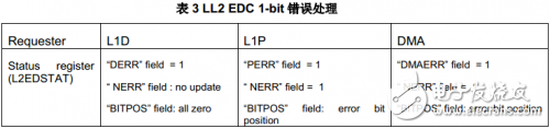
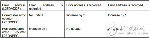
The error counter (L2EDCPEC, L2EDNPEC) is very useful for evaluating the type and probability of parity bit errors in long-running systems. The following table lists the details of the corresponding 2-bit error handling for different memory access requesters.
For errors greater than 2 bits, the EDC logic may detect and report a 1-bit or 2-bit error, or the EDC may not detect the error at all. Therefore, the KeyStone family of EDC hardware logic can only guarantee detection of 2-bit errors or correction of 1-bit errors.
Usually the probability of a soft error is very low. First, a 1-bit error occurs. After a relatively long time, the second error bit may be generated. Since the 1-bit error can be corrected and the 2-bit error cannot be corrected, we should correct the first bit error as much as possible before the second bit error occurs.
The operation of correcting 1-bit errors is often referred to as "refresh." To refresh a block of memory, you can use IDMA to set the source and destination addresses of the IDMA to the same address; the byte length is set to the block of memory that you want to overwrite. The address access must be 128-bit aligned, and the entire memory range must be an integer multiple of 128 bits. When IDMA reads data from LL2, the EDC hardware corrects the 1-bit error that may exist in the 128-bit word with valid check information. When IDMA writes the data back to the same address, EDC generates a checksum for the data and identifies it as valid.
The refresh operation is usually done in the 1-bit error interrupt service function. However, some data may not be accessed until a 2-bit error occurs after a 1-bit error occurs. 1-bit errors are not automatically reported when there is no access. To avoid this, the entire block of memory should be refreshed periodically to correct potential 1-bit errors. Below is an example of a code for a LL2 EDC refresh.

Usually, this function can be called in a timed interrupt. This function is called in a timed interrupt of 600 seconds.

In this way, the 1MB storage interval will be refreshed every 7 days. Because refresh operations compete with normal memory operations, they can affect the performance of normal memory operations. So the refresh operation can't be too frequent, but it must be done before the 2-bit error is generated. It must be weighed against the design. LL2 EDC Function Verification: The LL2 EDC logic can be halted by setting the SUSP bit in the L2EDCMD register. Using this feature, software can emulate EDC errors and verify EDC functionality. The code that verifies the LL2 EDC function is provided in the routine corresponding to this article, corresponding to the function LL2_ED_test().
3.3 SL2 error detection and correction
For basic information about the shared memory SL2, refer to "KeyStone Architecture Multicore Shared Memory Controller User Guide (SPRUGW7)". Check Bit Generation and Checking: There are two mechanisms for generating and detecting MSMC check information:
1. When writing to a 256-bit memory segment initiated by any master, the verification information is updated and set to be valid. A write operation of less than 256 bits invalidates the verification information. When the DSP master initiates a read operation of a 256-bit memory segment, the verification information is checked.
2. The MSMC contains a background error correction hardware called a refresh engine for periodically refreshing the contents of the memory. The number of refresh cycles can be configured by the REFDEL bit field in the SMEDCC register, and each refresh will read and write back a block of four 32-byte sizes. The refresh engine also reports an EDC error when detecting and correcting 1-bit or checking for a 2-bit error. Detailed descriptions of the mechanisms are provided in the MSMC User Manual.
After the DSP is reset, the MSMC hardware invalidates the verification information and reinitializes the verification information. When reading the MSMC memory for the first time, the software must first check the PRR bit in the SMEDCC (check the RAM for ready status information).
Error detection and correction configuration: The refresh engine of the SL2 EDC logic is enabled after the DSP reset, and the verification information is generated in the background. The software does not need to use DMA for memory refresh like the LL2 EDC. It only needs to query the PRR (Check RAM Ready) bit in the SMEDCC register to confirm that the check bit has been generated. In order to enable error correction, the ECM bits in the SMEDCC should also be enabled. Note that the error correction logic adds 1 cycle of latency to the read from SL2 (the access pipeline is increased by one level), but the access throughput does not decrease.
The following are the routines that enable the MSMC EDC function:

Error reporting mechanism: The MSMC user manual has detailed error reporting mechanism information. The following table is summarized here.
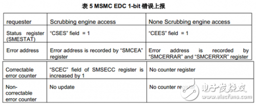
Note that the error address reported by the refresh engine is an address offset starting from 0, and the error address for a non-refresh access record is the SL2 address in the device starting at 0x0C000000.

MSMC EDC function verification: The MSMC EDC logic can be suspended by setting the PFn bit (bit0~3) in the SMEDCTST register. The address offset of SMEDCTST is 0x58. Each SL2 RAM bank corresponds to one bit in PFn (PF0~3 corresponds to banks0~3 in turn), and each bit can be used to disable the write operation to the check RAM. In this way, the check RAM corresponding to the bank can be frozen, so that the consistency of the SL2 stored content and the check information can be destroyed by deliberately injecting an error, thereby testing the detection correction logic. The specific order is as follows:
1. Write a known value to a location in the test bank so that a checksum can be correctly initialized for that location.
2. The PF corresponding to the SMEDCSTST is compared to the close-up 1 to freeze the check value.
3. Write an arbitrary byte to the above written position to change the value of the position. If the check function is checked, write a 1-bit difference value. If the test function is checked, write a value with a 2-bit difference. The checksum at this location is not synchronized with the value it stores.
4. Reading back the value of this location will result in a validation error of the selected type.
Corresponding code is provided in the routine corresponding to this article to verify the SL2 EDC function, and the corresponding function is SL2_EDC_test().
4 Other robust features
4.1 watchdog timer
For the basic knowledge of the watchdog timer, refer to the "Watchdog Timer Mode" section in the "KeyStone Architecture Timer64 User Guide (SPRUGV5)".
Timer 0~(N-1) can be used for N core watchdogs. In TCI6614, Timer 8 is the ARM watchdog timer. In watchdog mode, an event is generated when the timer counts down to zero. It is necessary for the software to write to the timer before the countdown is terminated, and then the count starts again. If the count reaches 0, a timer event is generated. The Watchdog Timer event can trigger a core reset, a device Reset, or an NMI exception, which can be selected by configuring the Reset Multiplex Register (RSTMUXx) as described in the appropriate device handbook.
Enables the watchdog event to trigger NMI exceptions with greater flexibility. In the NMI exception service function, the cause of the error and some critical status information can be recorded or reported to the host computer for fault analysis, and then if it If it is not self-healing, the device can be reset by software.
4.2 EDMA error detection
For basic EDMA CC error information, refer to the "Error Interrupts" section in the "KeyStone Architecture Enhanced Direct Memory Access (EDMA3) Controller User Guide (SPRUGS5)".
For basic EDMA TC error information, refer to the "Error Generation" section in the "KeyStone Architecture Enhanced Direct Memory Access (EDMA3) Controller User Guide (SPRUGS5)".
All EDMA error events can be routed as an exception to the CorePac. An event loss error is one of the most common EDMA CC errors, meaning that EDMA cannot complete the transfer of data as required, or an erroneous event triggers an EDMA transfer that should not be. A bus error is one of the most common EDMA TC errors and usually means that the EDMA has access to the wrong address (such as a reserved address or a protected address).
4.3 Interrupt Loss Detection
Loss or omission of interrupts is a common and often overlooked problem in real-time systems. Interrupt loss detection is an effective way to capture such anomalies. Refer to the “Interrupt Error Events†section of the “TMS320C66x DSP CorePac User Guide (SPRUGW0)†for basic interrupt loss detection information.
The software system should enable interrupt loss detection for interrupts that are routed to the DSP core and have corresponding software services. After all interrupts are configured, you can add the following code to enable interrupt loss detection:

Note that when interrupt loss detection is enabled and a breakpoint or single step is used for commissioning under CCS/Emulator, since the interrupt is not responded when the simulation is stopped, the probability of all interrupt loss errors reported at this time is high. If you want to ignore it, you can temporarily turn off interrupt loss detection for some or all of the interrupts during commissioning, but be careful not to forget to re-enable the feature in the officially released program.
5 exception handling
For basic information about exception handling, refer to the section "CPU Exceptions" in the "TMS320C66x DSP CPU and Instruction Set Reference Guide (SPRUGH7)".
For basic information about interrupt or exception event routing, refer to the "Interrupt Controller" chapter in the "TMS320C66x DSP CorePac User Guide (SPRUGW0)".
5.1 Exception Event Routing
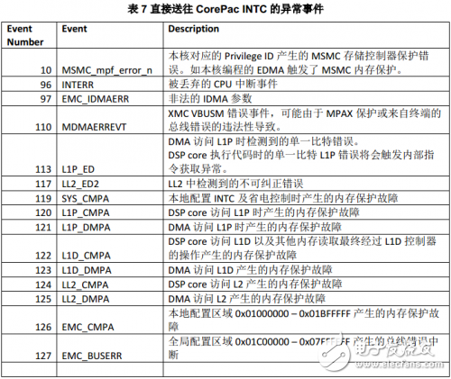
All error events originating from or triggered by CorePac are routed directly to the CorePac interrupt controller. The errors that are often treated as exceptions are shown in the following table.
Some other non-fatal error events, such as correctable LL2 EDC errors, should be routed to the interrupt instead of the exception. Error events originating from or triggered by shared modules in the device are routed to the CIC. The CIC basic information refers to the "KeyStone Architecture Chip Interrupt Controller (CIC) User Guide (SPRUGW4)".
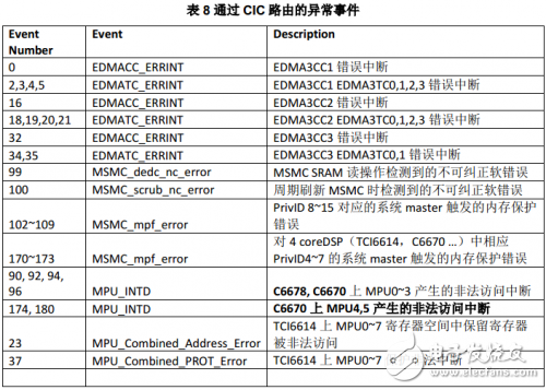
The events that are often treated as exceptions in CIC events are shown in the following table.
Each such exception can only be routed to one CorePac. Usually all of these events are routed to a CorePac. The following figure depicts the switches for DSP core internal control exception handling.
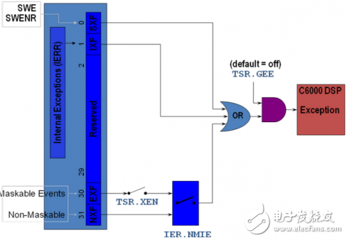
Figure 2 DSP core abnormal control switch
Once the software sets TSR.GEE and IER.NMIE, it can no longer be cleared by software and can only be cleared after reset. TSR.XEN can be set and cleared by software. XEN can be automatically cleared by hardware when entering the exception service function, and automatically restores the original state when exiting the exception service function. Therefore, by default, in the interrupt service function, TSR.GEE=1, IER.NMIE=1 and TSR.XEN=0.
5.2 Exception Service Function
The abnormal cause and related information should be recorded or reported in the abnormal function for fault analysis. The key record information is NRP. NRP is an exception return pointer and is usually used to determine where the exception is triggered. In fact, the delay between illegal operation and NRP capture is between 10 and 100 DSP Core cycles. The specific delay depends on many factors, such as the type of operation, the module that generates the abnormal event, and so on. For example, to perform a write operation to a MPU-protected register, the latency includes: a write instruction delay from the DSP core to the register; a routing delay of the error event from the MPU to the CIC and then to the CorePac exception module. Therefore, when we get NRP, we should search backwards from the location pointed to by NRP for about 10~100cycles to find the problematic operation.
However, some abnormal NRPs are meaningless, for example, for instruction fetch exceptions and illegal opcode exceptions. This usually happens when the program jumps to an illegal address, when the NRP also points to an illegal address. What we really want to know is what happened before the program jumped to an illegal address, but this could not be derived from the NRP. In this case, registers B3, A4, B4, B14 and B15 may be helpful. B3 may also hold the return pointer of the last function call; A4 and B4 may hold the parameters of the last function call; B15 is the stack pointer; B14 is the data pointer to some global variables. For more details, please refer to the section "7.4 Function Structure and Calling Conventions" in the "TMS320C6000 Optimizing Compiler User Guide (SPRUG187)". Based on this information, we may be able to deduce what happened before the program jumped to an illegal address. Note that B3, A4, B4 may have been modified to hold other information before the exception occurred, so they may not be useful. In fact, the probability that B3, A4, and B4 contain valuable information is still very high, so these registers are worth recording and analyzing.
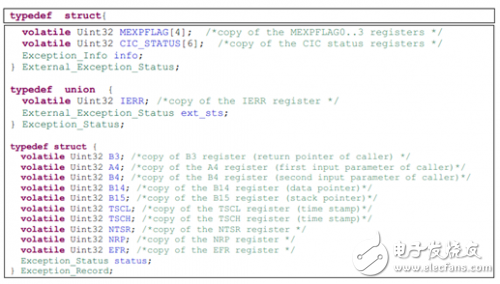
The value of the general-purpose register cannot be recorded in C code, but must be recorded in assembly code. The following example records the B3, A4, B4, B14, and B15 registers in "exception_record" and then calls "Exception_service_routine".

Other basic information that needs to be recorded is: EFR, IERR, NTSR, TSCL/TSCH.EFR is used to determine the type of exception: internal, external or NMI. For internal anomalies, the cause of the internal anomaly is recorded in the IERR. The NTSR records the DSP core state when an exception occurs. The recorded TSCL/TSCH is used to determine how long the device will run before the exception occurs.
For external exceptions, the cause of the exception is determined by examining the INTC and CIC flag registers. Corresponding to a specific exception, there are often specific status registers that can be checked, recorded, or reported. For example, if the memory protection is abnormal, the key information to be recorded is the fault address. Refer to the user guide for each module for more details on the status or logo.
Usually, the exception service function saves these exception information in a data structure similar to the following.
Information in these data structures can be passed to the host in an exception service function or exported for error analysis.
Usually the error handled by the exception service function is fatal and the user should not expect to return from the exception service function. In addition, the software does not always return safely from the exception service function, and the conditions that prevent safe return from exceptions are:
1. SPLOOPs that are abnormally terminated cannot be restarted correctly. You should verify that the SPLX bit value in the NTSR is 0 before returning.
2. An exception that occurs when the interrupt is blocked cannot be restarted correctly. You should verify that the IB bit value in the NTSR is 0 before returning.
3. An exception that occurs at a code that cannot be safely interrupted (such as a tight loop that protects multiple assignments) does not return correctly. The compiler usually closes the interrupt in these places in the code; see that the GIE bit value in the NTSR is 1 to verify that this condition is met.
4. NRP is not a legal address.
So usually the exception service function ends with a while(1) loop. By default, in the exception service program, TSR.GEE=1, IER.NMIE=1 and TSR.XEN=0. That is, NMI and internal exceptions are enabled in the exception service program.
When an enabled exception occurs in the first exception service routine, the program pointed to by the reset vector is executed. At this time, NTSR and NRP will not change. The TSR is copied to the ITSR, and the PC is copied to the IRP at this time. At this time, in order to avoid other external exceptions, the hardware sets the TSR to the default exception handling value, and the IER bit in the NMIE is cleared.
Usually the reset vector in the interrupt service table is jumped to the program start position such as _c_int00, so that the nested exception will restart the program. However, this is not what most users expect. What we usually expect is to end the program after the exception service has finished executing. In order to avoid a nested exception causing the program to restart, you can add an additional exception service to the nested exception. The user can modify the reset vector to jump to the nested exception service. In KeyStone devices, the loader does not depend on the reset vector starter, so modifying the reset vector does not affect the loading of the program.
6 routines
The related routines in this article can be run on the TCI6614 EVM, C6670 EVM and C6678 EVM. The following is the project directory structure:
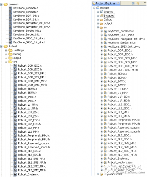
Figure 3 routine directory results
The "common" folder contains generic code such as DDR initialization and DMA, timers, multi-core navigators, SRIO drivers, and more. The memory protection initialization code, EDC, and exception handling code are included in KeyStone_common.c.
Each c file in the "src" folder contains a test case code. The main function is in "Robust_System.c". There are some macro switches at the beginning of "Robust_System.c", each of which is used to enable or disable a test case.

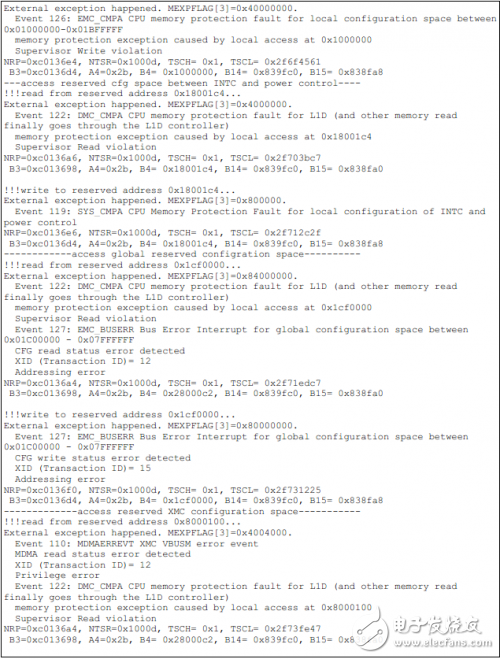
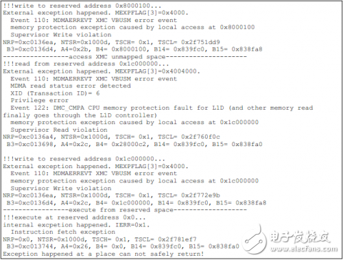
如果使能多个测试用例,æ¯ä¸ªç”¨ä¾‹ä¼šä¾æ¬¡æ‰§è¡Œã€‚由于程åºå¹¶ä¸èƒ½æ€»æ˜¯å®‰å…¨åœ°ä»Žå¼‚常æœåŠ¡ç¨‹åºä¸è¿”å›žï¼Œå› æ¤æœ‰å¯èƒ½åœ¨ä¸€ä¸ªæµ‹è¯•ç”¨ä¾‹åŽè¾“出如下信æ¯ï¼Œç„¶åŽæµ‹è¯•æµç¨‹è¢«ç»ˆæ¢ã€‚

如果出现这ç§æƒ…况,å¯ä»¥å…³é—这个测试用例然åŽé‡æ–°æµ‹è¯•å…¶ä»–的用例。在EVM上è¿è¡Œä¾‹ç¨‹çš„æ¥éª¤å¦‚下:
1.解压例程,将CCS workspace切æ¢åˆ°è§£åŽ‹åŽçš„文件夹;
2.在workspaceä¸å¯¼å…¥å·¥ç¨‹ï¼›
3.如果å‘生代ç 修改对工程é‡æ–°ç¼–译,也许需è¦åœ¨ç¼–译选项ä¸ä¿®æ”¹CSLä¿æŠ¤è·¯å¾„ï¼›
4.设置EVMæ¿ä¸Šçš„å™¨ä»¶åŠ è½½æ¨¡å¼ä¸ºNo boot模å¼ï¼›
5.将代ç åŠ è½½åˆ°DSP core0,è¿è¡Œï¼›
6.查看CCS stdout窗å£æµè§ˆæµ‹è¯•ç»“果。
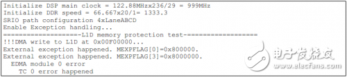
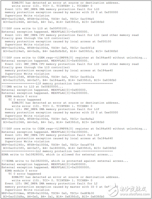
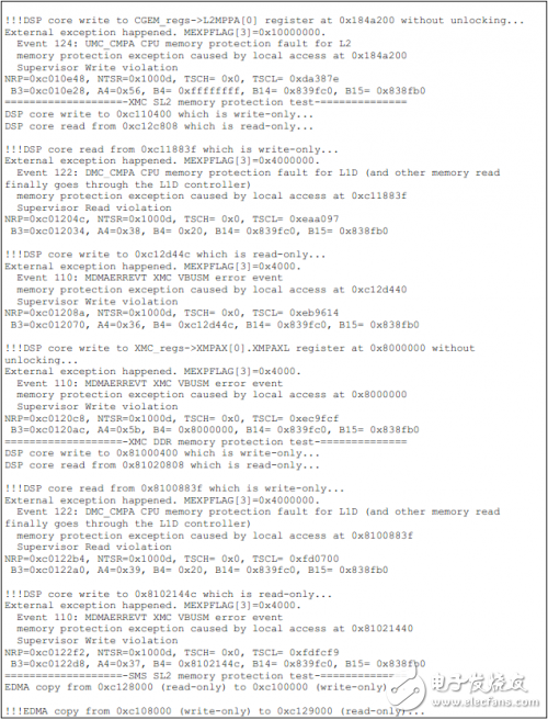
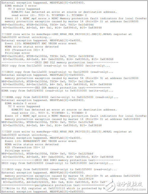
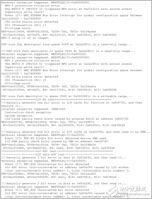
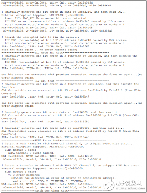
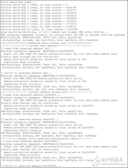
如下为TCI6614上的测试结果。
Installation Accessory,Encoder Sensor With Coupling,Encoder Sensor Wheel,Sensor Encoder
Yuheng Optics Co., Ltd.(Changchun) , https://www.yuhengcoder.com