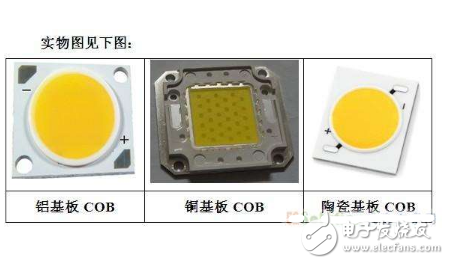
With the gradual maturity of the LED application market, users are increasingly demanding product stability and reliability, especially under the same conditions, requiring products to achieve better energy efficiency indicators, lower power consumption, and more competition. Product price. Based on this, compared with the traditional LEDSMD chip package and high power package, the on-chip (COB) integrated package technology directly encapsulates multiple LED chips on a metal-based printed circuit board as a lighting module directly through the substrate. Heat dissipation not only reduces the manufacturing process and cost of the bracket, but also has the advantage of reducing the thermal resistance of the thermal resistance, thus becoming a kind of packaging method promoted by the lighting enterprise.
In addition to good heat dissipation and low cost, COB light source can be personalized. However, in terms of technology, COB package still has shortcomings such as light decay, short life, and poor reliability. If it can be solved, it will be one of the leading directions for future package development.
COB performance is stable and widely usedCOB products are mainly used in the commercial lighting market. With the improvement of technology, the performance of high-power COB products tends to be stable, and has recently been gradually applied to outdoor lighting, including LED industrial and mining lamps, street lamps and other markets. Because high-power LEDs and COB LEDs have product design advantages and high light power that are not available in medium power, they will enhance the competitive advantage of the high-end lighting market.
First of all, in the high-end commercial lighting market, lighting is applied to markets such as museums and art galleries, mainly in downlights, projection lamps and reflector lamps. According to the data, in the global high-end commercial lighting market in 2016, 40% and 75% of the most widely used downlights and track spotlights use COB light sources (according to the number of lamps, mainly based on COB with power below 30W). ), and then grew at a compound growth rate of 11% and 6% respectively.
In addition, COB for vehicles is also one of the applications of COB. However, because the COB market itself is a small market with a small volume, and the vehicle COB is one of the branches of the niche market, the industry is less concerned. However, as many COB manufacturers began to cut into the automotive COB market on a large scale, the COB for vehicles quickly became the main battlefield for price wars. Zheng Haibin, deputy general manager of Zhaochi Energy, said that the price/performance ratio is king. He does not agree with this view. He believes that the COB for vehicles is mainly the aftermarket, and the entry threshold is relatively low, and the price competition is relatively normal. For any market, as long as you enter the product standardization stage, it can be called the Red Sea market.
In addition, industrial lighting brings new opportunities to small and medium-sized COB companies. According to the survey data, LED industrial lighting will grow rapidly in the next few years. In 2016, the LED industrial lighting market will reach 2.932 billion US dollars. After that, it will grow at a rate of more than 16% per year. In 2016, the growth rate is as high as 24% to 2018. In the year, the market size will reach 3.935 billion US dollars. At the same time, because most of the industrial lighting is invisible engineering channels, you can avoid the price war and the scale of war.
Analysis of advantages and disadvantages of COB packagingThe application of COB package has been applied in the field of lighting for many years. It has many advantages in various aspects, so it has been favored by many lighting companies. So what kind of spark will COB packaging technology be applied to the display screen? Will there be some levels of acclimatization? Let's analyze the advantages and disadvantages of COB packaging. It is understood that COB packaging technology is applied to the display screen, which has the incomparable advantages of traditional packaging technology.
1. Ultra-thin: According to the actual needs of customers, PCB board with thickness from 0.4-1.2mm can be used to reduce the weight to 1/3 of the original traditional products, which can significantly reduce the structural, transportation and engineering costs for customers.
2. Anti-collision and compression: The COB product directly encapsulates the LED chip in the concave lamp position of the PCB board, and then is encapsulated and cured with epoxy resin glue. The surface of the lamp point is convex into a spherical surface, smooth and hard, and is resistant to collision and wear. .
3. Large viewing angle: The COB package uses shallow well spherical illumination, the viewing angle is greater than 175 degrees, close to 180 degrees, and has a better optical diffuse color dimming effect.
4. Bendable: The bendability is unique to the COB package. The bending of the PCB does not cause damage to the packaged LED chip. Therefore, the COB module can be used to easily make LED curved screens, circular screens, and waves. Shape screen. It is an ideal substrate for personalized screens in bars and nightclubs. It can be seamlessly spliced, the production structure is simple, and the price is far lower than the LED shaped screen made by the flexible circuit board and the traditional display module.
5. Strong heat dissipation: COB products are packaged on PCB board, the heat of the wick is quickly transmitted through the copper foil on the PCB board, and the thickness of the copper foil of the PCB board has strict technical requirements, plus immersion gold. The process hardly causes severe light attenuation. Therefore, there are very few dead lights, which greatly extend the life of the LED display.
6, wear-resistant, easy to clean: the surface of the lamp point is convex into a spherical surface, smooth and hard, collision-resistant and wear-resistant; there are dead spots, you can repair point by point; no mask, dust can be cleaned with water or cloth.
7, all-weather excellent characteristics: the use of triple protection treatment, waterproof, moisture, corrosion, dust, static electricity, oxidation, UV effect is outstanding; to meet all-weather working conditions, the temperature difference of minus 30 degrees to zero 80 degrees can still be used normally.
To put it bluntly, the advantages of the COB display package are really quite a lot, especially when compared with the traditional package form, the contrast effect is more obvious. Since there are many advantages, why not get a large-scale application in the early development of LED display? What are the inadequacies of COB packaging? Hu Zhijun, deputy general manager of Shenzhen Weiqiaoshun Optoelectronics Co., Ltd. said: "The only shortcoming of COB packaging is that the screen ink color is not well controlled, that is, when the lamp is not lit, the surface ink color is inconsistent." Shenzhen Aolida Technology Co., Ltd. Yang Rui, the company's marketing director, said frankly: "The scarcity of the COB display package is that the surface consistency is not enough. If this problem is not solved, it will be difficult to get the customer's approval."
The COB packaging technology is categorized as a package-free or provincial-saving package. However, this package does not eliminate the packaging process, but saves the packaging process. Compared with the SMT process, the COB packaging process is saved. Going to a few steps saves time and process to a certain extent, and also saves costs to a certain extent. SMD's production process needs to undergo solid crystal, wire bonding, dispensing, baking, stamping, splitting, color separation, tape, and patch. The COB process is simplified on this basis. First, the IC is attached to the circuit board. Then solid crystal, wire bonding, testing, dispensing, baking, and become a finished product.
In terms of the production process alone, several steps have been omitted, and industry insiders say that this can save a large part of the cost. It is worth noting that the COB package does not require reflow soldering, which is one of the advantages of COB. Array's marketing director Yang Rui said that the conventional package is to place the lamp bead on the PCB for soldering. When the lamp is getting denser and denser, the lamp pin will become smaller and smaller, so the precision of soldering will be higher. How many lamps in a square, one lamp has four feet, then there will be many solder joints in one square. At this time, the requirements for solder joints are very high, then the only solution is to reduce the solder joints. Very small solder stability is very poor, it may be accidentally touched, it may fall off, this is a problem that SMD can not avoid; COB package eliminates the process of splitting, color separation, drying, etc. The most critical difference is to remove the solder. Process, SMD in the process of soldering, the temperature control is extremely difficult to master, the temperature is too high, will cause damage to the lamp, too low, the solder does not completely melt. It is easy to cause the phenomenon of virtual welding, false welding, etc., which is a great challenge to the stability of the lamp bead. And COB does not have this process, then the stability will be greatly improved.
The processing technology of the traditional LED display screen is quite numerous, especially in the process of reflow soldering. Under the high temperature state, the expansion coefficient of the SMD lamp bead holder and the epoxy resin is different, which easily causes the bracket and the epoxy resin encapsulation to fall off. In the gap, the dead light phenomenon gradually appears in the later use, resulting in a high defect rate. The reason why the COB display is more stable is because there is no reflow soldering lamp in the processing technology. Even if there is a post-reflow soldering IC process, the diode chip has been cured and cured with epoxy resin, thus avoiding soldering. There is a problem of gaps between the lamp holder and the epoxy resin caused by high-temperature soldering in the machine.
COB packaging challengesThe emergence of a new product and new technology and new technology will never go smoothly. It is necessary to continuously test in the R&D and production process, and constantly try to find the problem, in order to solve the problem in real time. The emergence of each problem is the process of research and development personnel, in this process, full of hardships, but also accompanied by achievements and satisfaction. The development of all new things is perfected little by little, and it is also close to success step by step. But for now, the development of COB packaging technology can not be called mature, after all, the development of new things still takes time. At this stage, COB packaging technology still faces some challenges, and these challenges are gradually improved in the continuous efforts of enterprises. It is understood that at present, COB packaging technology currently has three challenges.
1. One pass rate of the packaging process
COB package method Because of its characteristics, COB package is to be on a large board. This board has a maximum of 1024 lights. If SMD seals a lamp, you only need to change one, but the COB package is 1024. After the lamp package is completed, the test is performed, and all the lamps are confirmed to have no problem before the seal can be applied. How to ensure that the entire board of 1024 lights is completely intact, one pass rate is a very big challenge.
2, the finished product pass rate
The COB product is first sealed. After the lamp is sealed, the IC driver device is subjected to a reflow process. How to ensure that the lamp surface is over-reflowed, the high temperature of 240 degrees in the furnace does not damage the lamp. This is another big challenge. Compared with SMD, COB saves the surface reflow soldering process, but the device surface needs to be reflow soldered like SMD, which means that SMD has to be reflowed twice. When SMD is reflowed, the temperature in the furnace will cause two kinds of damage to the lamp surface. One is the wire. If the temperature is too high, it will rapidly expand rapidly, which will cause the filament to break. The second one is The heat in the furnace is quickly transmitted to the wick through the four pins of the bracket. The wick may cause small fragmentation damage. This damage is fatal, and the detection is often difficult to detect, including aging tests, but it is difficult to detect, but This tiny damage of the crystal is finely cracked after a period of time
Use, this drawback will be highlighted, which will lead to the failure of the lamp. The COB is to ensure that when the lamp surface is over-reflowed, the high temperature in the furnace does not cause damage to it, and the yield is guaranteed. This is also a very important aspect.
3, the whole lamp repair
For the maintenance of COB lamps, professional maintenance and maintenance are required. One of the biggest problems with single-lamp maintenance is that after repairing, a circle will appear around the lamp, and a lamp will be repaired. The surrounding circle will be smoked by the welding torch, and the maintenance difficulty is relatively high.
If there are challenges, it is necessary to find a corresponding solution. At present, the problems encountered in the packaging and maintenance process of the COB package are solved by the enterprise. For example, when the lamp surface is over-reflowed, a certain solution is adopted. The way to protect the lamp surface to reduce damage; the point-by-point correction technology is used in the maintenance process to ensure the consistency between the lamp beads.
CIXI LANGUANG PHOTOELECTRIC TECHNOLOGY CO..LTD , https://www.cxblueray.com