In December 2017, the Shanghai Microtechnology Industry Research Institute (SITRI), which is dedicated to the innovation platform of “Beyond Moore†industry, officially released the HV600/HV650 series of 8-inch silicon-based GaN epitaxial wafer products for surface-to-air applications. The wafer product has high crystal quality, high material uniformity, high withstand voltage and high reliability. At the same time, the effective life of the material exceeds 1 million hours, which successfully solves the technical problem that plagues the application of silicon-based GaN materials. Industrial application of medium and high voltage silicon-based GaN power devices.
Compared with traditional semiconductor materials, the third-generation semiconductor material GaN has outstanding advantages such as wide band gap, high saturation carrier speed, high breakdown electric field, high temperature resistance and radiation resistance, and is suitable for a new generation of high-speed, high-efficiency power devices. Manufacturing, in the field of wireless charging, fast charging, cloud computing, 5G communications, laser radar, new energy vehicles and other fields have broad application prospects. At the same time, silicon-based GaN materials have significant cost advantages, and in the case of using large-sized silicon wafers as epitaxial substrates, low-cost manufacturing comparable to conventional silicon-based power devices can be achieved. Therefore, silicon-based GaN technology is also considered to be the mainstream technology of new power electronics.
The Power Devices Division of Shanghai Microtechnology Industry Research Institute was established in 2016 to develop silicon-based gallium nitride materials and devices for industrial applications. In the recent "3rd National Symposium on New Semiconductor Power Devices and Application Technologies", Dr. Yuan Li, Director of Power Devices Division, introduced the latest development of the 8-inch silicon-based GaN epitaxial material project of Shanghai Microtechnology Industry Research Institute. The high reliability and uniformity of the HV600/HV650 series of 8-inch silicon-based GaN epitaxial wafer products has received wide attention and high praise from the participants.
Epitaxial structure conforming to 8-inch silicon process line
Shanghai Microtechnology Industry Research Institute HV600/HV650 series silicon-based GaN materials use a low-resistance 8-inch silicon substrate to solve the thermal mismatch problem between silicon substrate and GaN through pre-strain technology, and select the appropriate epitaxial layer structure according to application requirements. .
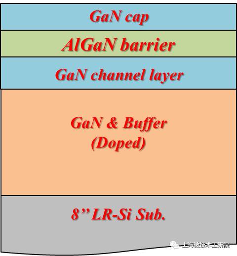
Figure 1: Schematic diagram of the epitaxial structure of HV600/HV650 series materials
Excellent material quality
To meet the 600 V/650 V withstand voltage requirements, Shanghai Microtechnology Industry Research Institute uses thick film epitaxial growth technology over 4 microns. The optimized GaN epitaxial crystal growth control solves the problems of wafer warpage and crystal quality defects caused by lattice mismatch between GaN and silicon materials. The HV600/HV650 series materials are crack-free, low warpage (≤ ± 50 μm) and low surface roughness (≤ 0.3 nm), meeting the mass production requirements of 8-inch power devices.
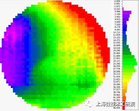
Figure 2: Wafer warpage of HV600/HV650 series materials
Low defect density
HV600/HV650 adopts optimized GaN epitaxial defect control technology to achieve high dislocation density and high crystal quality while achieving high withstand voltage and thick film growth. Its XRD (002/102) half height and width are less than 400/500 arcsecs respectively. .
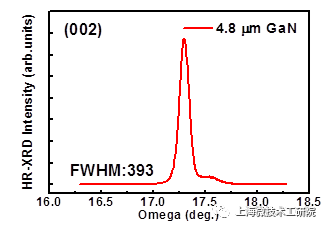
Figure 3: HV600/HV650 Series Material HRXRD GaN (002)
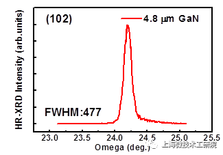
Figure 4: HV600/HV650 Series Material HRXRD GaN (102)
Excellent material uniformity
The HV600/HV650 series products have excellent material uniformity. The thickness of the 8-inch material epitaxial layer and the Al variance of the AlGaN barrier layer are less than 0.3% and 2%, respectively, ensuring high uniformity and high yield in mass production of large-size silicon-based GaN power devices, overcoming silicon-based Bottlenecks in the industrial application of GaN devices.
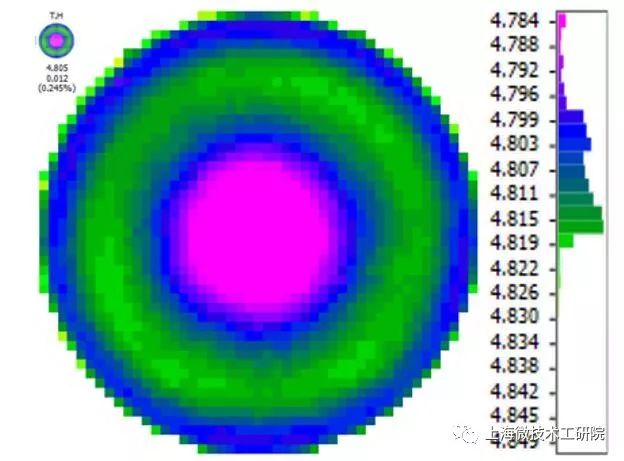
Figure 5: Epitaxial thickness distribution of HV600/HV650 series materials
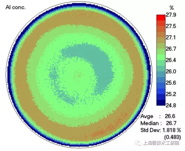
Figure 6: Al component distribution of AlGaN barrier layer in HV600/HV650 series materials
Abundant pressure resistance
For high-voltage applications in 600 V/650 V, the HV600/HV650 series have ample pressure capability. Based on the industry's stringent standards of leakage current of 1 μA/mm2, the HV600/HV650 has a vertical withstand voltage of 640/700 V. With the same stringent leakage current of 0.1 μA/mm as the criterion, the HV600/HV650 has a lateral withstand voltage of 700 V/760 V when the substrate is grounded, and a lateral withstand voltage of 950 V/1010 V when the substrate is floating. Meet the needs of 600 V / 650 V applications.
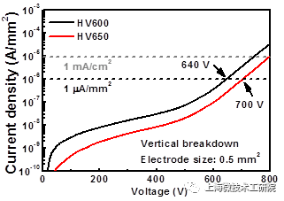
Figure 7: Vertical withstand voltage characteristics of HV600/HV650 series materials
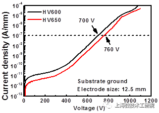
Figure 8: Transverse withstand voltage characteristics of HV600/HV650 series materials (substrate ground)
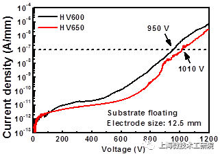
Figure 9: Transverse withstand voltage characteristics of HV600/HV650 series materials (substrate floating)
Good forward conduction characteristics
The HV600/HV650 series materials have good forward conduction characteristics, and the two-dimensional electron gas concentration is greater than 9x10^12 cm^(-2), the two-dimensional electron gas mobility is greater than 1800cm2/V·s, and the sheet resistance is less than 400 Ω/sq. .
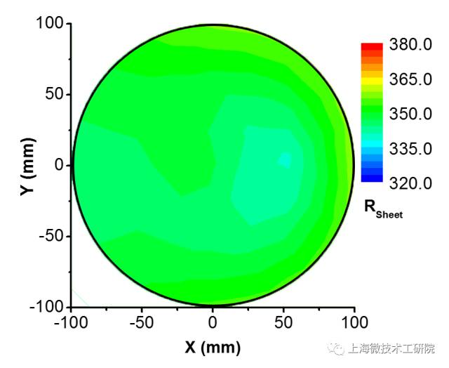
Figure 10: Square resistance distribution of HV600/HV650 series materials
High reliability material
Based on optimized silicon-based GaN epitaxial growth technology, the HV600/HV650 series products have excellent material reliability. According to the high pressure TDDB test, the HV600/HV650 series materials have an effective life of more than 1,000,000 hours (114 years) at nominal pressure.

Figure 11: Longitudinal high voltage TDDB test
At the same time, HV600/HV650 series materials also have excellent high temperature resistance. At 150 oC and substrate grounding, the lateral leakage of the 600 V/650 V products is 0.7 and 0.6 μA/mm, respectively, both less than 1 μA/mm. It ensures the high efficiency and safety of materials in the common temperature zone of power devices.
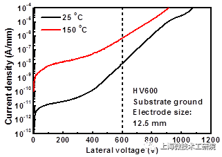
Figure 12: Transverse voltage withstand characteristics of HV600 series materials at high temperature (substrate ground)
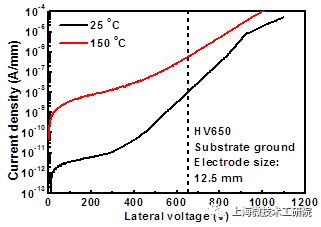
Figure 13: Transverse withstand voltage characteristics of HV650 series materials at high temperature (substrate ground)
The HV600/HV650 series of 8-inch silicon-based GaN epitaxial wafer products successfully developed by Shanghai Micro-Technology Research Institute broke through the material bottleneck of mass production of silicon-based GaN devices, and achieved the first high reliability in the industry with more than 1 million hours. . At the same time, the HV600/HV650 series also has small-sized epitaxial wafers such as 6-inch, which meets the industry's demand for silicon-based GaN epitaxial materials of various sizes.
WiFi Camera Module is your popular hidden camera that can be used anywhere to help you. This hidden camera can be used not only at home, but also at work or elsewhere.
WiFi camera is the product of modern high-tech, also known as micro monitor, which has the characteristics of small size, powerful function and good concealment.
WiFi cameras are widely used, suitable for aviation, commerce, media, enterprises and institutions, families and other industries. The emergence of miniature cameras brings convenience to people's lives, and at the same time, some phenomena related to corporate secrets and personal privacy also arise.
WiFi Camera Module,hidden camera for house,hidden camera house,hidden camera with audio,hidden camera in house
Jingjiang Gisen Technology Co.,Ltd , https://www.gisentech.com