In recent years, with the rapid development of wireless communication technology towards high frequency and high speed, and the development of electronic components towards miniaturization and low power consumption, based on Film Bulk Acous Tec Resonator (FBAR) The research and development of filters has attracted more and more attention.
Conventional wireless communication systems often use dielectric filters and SAW (Surface Acous Wave Wave) filters. Although the dielectric filter has better performance, it is bulky and inconvenient to use in portable devices. The SAW filter is small in size and widely used at present, but still has low operating frequency, large insertion loss, and relatively high power capacity. The FBAR filter not only combines the advantages of superior dielectric ceramics and small SAW volume, but also overcomes the shortcomings of both. It has small volume, high Q value, high operating frequency, large power capacity and low loss. The next-generation filter that replaces the SAW filter is also the filter that is considered by the industry to be the most likely to fully integrate the RF module.
FBAR filter history backgroundThe name FBAR is derived from the bulk acoustic wave (BAW, Bulk AcousTIc Wave). The concept of BAW was proposed in the 1960s, but it was not until 1980 that Lakin and Wang first made thin-film resonators with a fundamental frequency of 435 Mhz on Si chips. In 1990, Krishnaswamy and Rosenbaum extended the FBAR structure filter to the Ghz band for the first time.
Subsequently, after 10 years of research, Agilent finally succeeded in developing a film cavity acoustic resonance filter (size 5.8*11.8*1.8) applied to the US PCS1900MHz frequency band in 1999, and officially proposed the title of FBAR. And in 2001 it will mass production. Subsequently, the US TFR company, Germany's Infineon (Infineon) and South Korea's ANT company have also launched their own FBAR products. In 2002, Agilent FBAR sales exceeded 20 million. Agilent's success in the FBAR market has led to the rapid development of FBAR technology. In 2005, Agilent officially changed its name to Avago due to strategic adjustments, and broke through 200 million shipments the following year, which is a memorable milestone for Avago.
The great success of Agilent and Avago in the FBAR filter market has rapidly driven the development of FBAR technology. Later, Infineon, Philips, Fujitsu Media Device and Ube Industries Co., Ltd. also launched their own FBAR filter products. German market research firm Wicht Technologie ConsulTIng (WTC) has made a very optimistic estimate of the market prospects of FBAR in the coming years.
FBAR filter worksFBAR is a resonance technique based on bulk acoustic wave (BAW), which uses the inverse piezoelectric effect of a piezoelectric film to convert electrical energy (signal) into sound waves to form a resonance.
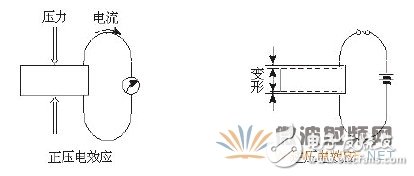
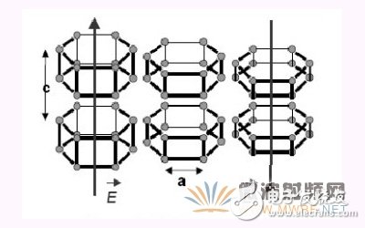
As shown in the figure, when a constant electric field is applied to both ends of the material, the deformation of the material changes with the magnitude of the electric field, and when the direction of the electric field is reversed, the direction of deformation of the material also changes. "When an alternating electric field is added, the direction of deformation of the material changes with the contraction or expansion of the positive and negative half cycles of the electric field." This is called the inverse piezoelectric effect.
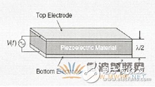
Typical structure diagram of FBAR resonator
Unlike SAW, this vibration occurs in the body cavity of a piezoelectric material and therefore can withstand greater power. This is one reason why FBAR technology is superior to SAW.
Vibration of a piezoelectric film layer under an alternating electric field
Such vibrations excite a bulk acoustic wave propagating along the thickness direction of the film (C-axis), which is transmitted back to the interface between the upper and lower electrodes and the air, and then reflected back and forth inside the film to form a shock. A standing wave oscillation is formed when the acoustic wave propagates in the piezoelectric film exactly at an odd multiple of a half wavelength.
V=f*λ=f*2d, since the wavelength of the acoustic wave is much shorter than the electromagnetic wave, the resonator formed by the acoustic wave at the point frequency will be several orders of magnitude smaller than the resonator formed by the electromagnetic signal, and d is the piezoelectric layer. Thickness, it can be seen that the thickness of the piezoelectric layer is generally less than a few microns. In the SAW process, the finger width and the gap of the interdigital electrode are inversely proportional to the operating frequency, which increases the difficulty of lithography and limits the frequency of use.
Sound waves form series resonance in the upper and lower bounds
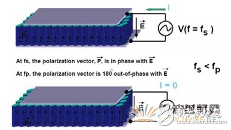
Under the action of an alternating voltage V(fs), the polarization vector P is in phase with the electric field E, and the acoustic wave forms a series resonance in the upper and lower boundaries. At this time, the electrical impedance of the bulk acoustic wave resonator is at a minimum.
Under the action of an alternating voltage V(fp), the polarization vector P and the electric field E are opposite phases, and the acoustic wave forms a parallel resonance in the upper and lower boundaries. At this time, the electrical impedance of the bulk acoustic wave resonator is at a maximum. The acoustic wave loss at the frequency fp is the smallest, so the acoustic signal can be transmitted smoothly.
In addition to the resonant frequency f(fs, fp) described above, there are effective electromechanical coupling coefficients Keff2 and quality factor Q, which are defined as:
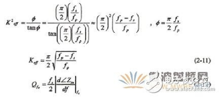
The effective electromechanical coupling coefficient Keff2 is used to represent the relative frequency of the series resonant frequency fs of the bulk acoustic resonator and the parallel resonant frequency fp, and also represents the bandwidth of the bulk acoustic wave resonator filter. The larger the Keff2, the bandwidth of the filter formed by the resonator. The larger, Keff2 is mainly determined by the material parameters of the piezoelectric film.
The quality factor (Q) can be used to determine the acoustic wave loss of the resonator; there are two main reasons for the loss of sound waves:
The first is the quality of the film itself. In general, thin films with poor quality will have high stress, high density of grain boundaries and a large number of defects and impurities, which will cause scattering of sound waves, thus reducing quality factors. The material with high acoustic wave velocity has a high quality factor because the sound wave is not easily absorbed when it is transmitted.
The second is the surface roughness of the film. The surface roughness of the electrode and the piezoelectric film is large, which causes scattering loss of sound waves and electrical loss of the electrodes, which causes a decrease in quality factors. Therefore, for the bulk acoustic wave resonator component, as long as it is the path of acoustic wave transmission, whether it is a piezoelectric layer or a reflective layer, the growth quality of each layer of the film affects the quality factor of the overall component.
Three FBAR structuresThere are three main types of mainstream FBAR structures: air gap type, silicon back type etching type and solid state assembly type.
1, air gap type
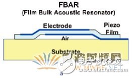
This FBAR is a MEMS-based surface micromachining that forms an air gap on the upper surface of the silicon wafer to limit the acoustic waves within the piezoelectric oscillator stack. The air chamber is prepared by first filling the sacrificial material and then removing it to form an air-metal interface. This method is compatible with traditional silicon art.
2, silicon reverse etching type
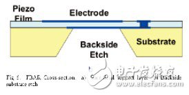
This FBAR is a MEMS-based bulk silicon micromachining technique that etches the opposite side of the Si wafer. An air-metal interface is formed on the lower surface of the piezoelectric oscillating stack to limit the acoustic waves within the piezoelectric oscillating stack. A disadvantage of this technique is that the mechanical fastness is lowered due to the large area removal of the Si substrate.
3, solid-state assembly structure
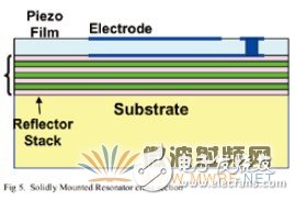
This type of FBAR uses Bragg's reflective layer technology to limit the acoustic waves within the piezoelectric oscillator stack. It consists of a layer of quarter-wavelength high acoustic impedance material and a quarter-wavelength thickness of low acoustic impedance material. The larger the number of layers, the larger the reflection coefficient, and the higher the Q value of the fabricated device. However, the reflection effect is not as good as the reflection effect of the first two structures anyway. Therefore, the Q value of the FBAR based on the Bragg reflection layer is not as good as the first two. High.
Preparation of FBAR devicesThe ideal air gap type FBAR is a sandwich structure, that is, an upper electrode/piezoelectric layer/lower electrode, and an air gap is etched between the silicon surface and the lower electrode surface of the FBAR to form an air interface. The actual air-gap FBAR resonator includes an upper electrode/piezoelectric layer/lower electrode/support layer, and an air gap is etched between the silicon surface and the lower surface of the support layer to form an air interface, thereby forming an air interface on the FBAR substrate. An air reflecting layer is formed to form a standing wave between the two air interfaces to confine the acoustic energy to the FBAR substrate.
Let us look at the preparation process of the air gap FBAR device.
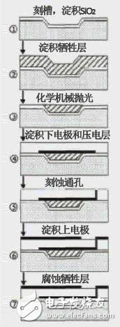
1. Etch a groove (air gap) on the surface of the prepared silicon wafer, and then deposit a thin SiO2 buffer layer to protect the silicon substrate.
2. Fill the sacrificial layer, such as Ti, phosphor quartz glass PSG
3. Use chemical mechanical polishing of the surface to remove excess sacrificial layers
4. Depositing the lower electrode, photolithography into the desired pattern, and then depositing a high C-axis oriented piezoelectric film ALN by reactive RF magnetron sputtering
5. Etching the piezoelectric film using RIE etching to form a via that leads the bottom electrode
6. Deposit the upper electrode and lithography to form the desired pattern
7. Corrosion removes the sacrificial layer to form an air gap
Material analysis for FBAR
At present, the materials used in the FBAR piezoelectric film are mainly ALN, ZnO and PzT, the materials of the metal electrodes are Mo, A1, etc., and the materials of the Bragg reflection layer are w, si02, ALN and the like.
There are several parameters that must be considered when choosing a material for a piezoelectric film:
Table 1 Piezoelectric material parameter table
Tab.1 Comparison of piezoelectric materials for FBAR
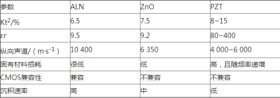
(1) The piezoelectric coupling coefficient Kt determines the conversion ratio between electrical energy and mechanical energy, and also determines the bandwidth of the RF filter based on FBAR.
(2) The relative dielectric constant εr, together with the electrode area and the thickness of the piezoelectric film, determines the electrical impedance value of the FBAR, and the high dielectric constant can reduce the size of the FBAR.
(3) Sound velocity v. According to v=f*λ, the smaller the speed of sound, the smaller the thickness and size of the device.
(4) Material inherent loss. The loss of the filter is small, and the insertion loss of the filter is also small. At present, ALN and ZnO have been successfully applied to the FBAR filter, and the PzT-based FBAR filter has not been commercialized due to excessive loss. The ALN loss is minimal.
(5) Temperature coefficient. The temperature coefficient affects the drift of the oscillation frequency with temperature. The temperature coefficient of ALN is much lower than that of ZnO.
(6) Thermal conductivity. The high thermal conductivity results in a large power capacity. ALN has excellent thermal conductivity.
(7) Chemical stability. Chemical stability affects the reliability of the device in humid environments, and ALN is much more stable than ZnO.
In addition, materials such as zinc, lead, and zirconium are very dangerous materials for CMOS processes because they severely reduce the lifetime of carriers in semiconductors, and ALN does not have this problem.
The preparation of the film is also a problem that cannot be ignored. Therefore, considering various aspects, ALN is a suitable piezoelectric material, although it does not look like ZnO and PZT at first glance.
As for the selection of the electrode material, ZnO is superior to AL on the principle of low loss and high sound velocity, and an amorphous layer like the AL and ALN film is not formed between the ZnO and ALN films.
ConclusionIn recent years, with the improvement of the preparation methods of piezoelectric thin film materials and the development of semiconductor process technology, FBAR related technologies have also developed rapidly. FBAR can be made into a variety of RF integrated microwave devices and high-sensitivity sensors such as high-performance filters, duplexers, and oscillators. FBAR is currently the only RF filter solution that can be integrated with RFICs and MMICs, and FBAR offers more profitable performance at a lower price and is highly competitive in the market. In the next generation of wireless communication systems and wireless access, FBAR devices will have a broader market prospect.
We are manufacturer of Ev Car Chargers in China, if you want to buy Level 2 Ev Charger,Evse Charger,Portable Charging Station please contact us.
Ev Car Chargers,Level 2 Ev Charger,Evse Charger,Portable Charging Station
Shenzhen Hongjiali New Energy Co., Ltd. , https://www.hjlcharger.com