Function:Clock,Calendar,Alarm
Package/Box: eDIP
Time format: HH:MM:SS, Binary
Date format: DW:DM:M:Y, Binary
RTC storage capacity: 113B
Supply Voltage (Max): 5.5V
Supply voltage (min): 4.5V
Maximum operating temperature: +70C
Minimum operating temperature: 0C
Installation style: Through Hole
RTC bus interface: Multiplexed
DS12C887 device features· Calculate seven kinds of calendar information in seconds, minutes, hours, weeks, days, months, and years before 2100 and take leap year compensation;
· Comes with a crystal oscillator and a lithium battery. Can work for 10 years without external power supply;
• For the time of day record, there are two modes, 12-hour and 24-hour. In the 12-hour mode, AM and PM are used to distinguish between morning and afternoon;
· Optional daylight saving mode
There are two ways to represent time: one is represented by a binary number, and the other is represented by a BCD code;
DS12C887 with 128 bytes of RAM, 11 bytes used to store time information, 4 bytes of RAM used to store DS12C887 control information, known as the control register, 113 bytes of RAM for users to use;
Data/address bus multiplexing
User programmable to achieve a variety of square wave output
· Can be applied to both MOTOROLA and INTEL buses. - I only describe the INTEL bus implementation method here
· Three kinds of programmable interrupts: fixed alarm interrupt, clock update end interrupt, periodic interrupt
DS12C887 pin and function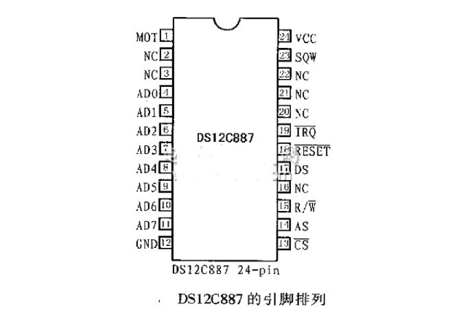
GND, VCC: DC power supply, where VCC is connected to the +5V input and GND is grounded. When the VCC input is +5V, the user can access the data in the RAM in the DS12C887 and can read and write the data. When the VCC input is less than When +4.25V, the user is prohibited from reading or writing internal RAM. At this time, the user cannot correctly acquire the time information in the chip. When the input of VCC is less than +3V, DS12C887 will automatically switch the power supply to the internal lithium battery. In the pool, to ensure that the internal circuits can work properly.
MOT: Mode selection pin, DA12C887 has two operating modes, Motorola mode and Intel mode. When MOT is connected to VCC, the selected working mode is Motorola mode. When MOT is connected to GND, the Intel mode is selected. This article focuses on Intel mode.
SQW: square wave output pin. When the supply voltage VCC is greater than 4.25V, the SQW pin can be used for square wave output. At this time, the user can obtain 13 types of square wave signal output by programming the control register.
AD0 ~ AD7: Multiplexes the address data bus, this bus adopts the time division multiplexing technology, in the first half of the bus cycle, it is the address information that appears on AD0- AD7, can use to strobe the RAM in DS12C887, the second half of bus cycle Part of the data appears on AD0 ~ AD7.
AS: Address strobe input pin. During read and write operations, the rising edge of AS latches the address information appearing on AD0~AD7 to DS12C887, and the next falling edge clears the address information on AD0~AD7, regardless of whether Effective, DS12C887 will perform this operation. DS/RD: Data selection or read input pin. This pin has two operating modes. When MOT is connected to VCC, Motorola operating mode is selected. In this working mode, the DS of the rear part of each bus cycle is high power. Flat, known as data strobe. During a read operation, the rising edge of DS causes the DS12C887 to send internal data to buses AD0 through AD7 for external reads. During a write operation, the falling edge of DS will latch the data on AD0~AD7 in DS12C887. When MOT is connected to GND, the Intel operating mode is selected. In this mode, this pin is the read enable input pin, ie ReadEnable. .
R/W: Read/write input. This pin also has two operating modes. When MOT is connected to VCC, R/W operates in Motorola mode. At this time, the function of this pin is to distinguish between read operation and write operation. When R/W is high, it is a read operation. When R/W is low, it is a write operation. When MOT is connected to GND, the pin is Work in Intle mode, this time as a write enable input, that is WriteEnable.
CS: chip select input, active low.
IRQ: Interrupt request input, active low, this pin has no effect on the contents of the clock, calendar, and RAM in the DS12C887. It only affects the internal control registers. In a typical application, RESET can be directly connected to VCC. This ensures that the DS12C887's internal control registers are not affected when power is lost.
There are 11 bytes of RAM in the DS12C887 to store time information and 4 bytes to store control information. The specific scale addresses and values ​​are listed in Table 1. Can be found out from Table 1: There are 4 control registers such as AB of the control register inside DS12C887, users can visit it at any time to carry on control operation to DS12C887.
About DS12C887 access by external RAM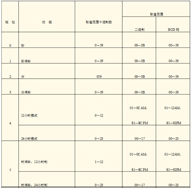
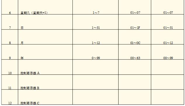
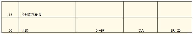
Table 1 DS12C887 storage function
Can be found out from Table 1: There are 4 control registers such as AB of the control register inside DS12C887, users can visit it at any time to carry on control operation to DS12C887.
Address function value range decimal number
Binary BCD code
0 seconds 0 to 5900 to 3B00 to 59
1 second alarm 0 to 5900 to 3B00 to 59
2 points 05900~3B00~59
3 minutes alarm 0~5900~3B00~59
12 hours mode 0 ~ 1201 ~ 0CAM,
81~8CPM
01 to 12 AM,
481~92PM
24-hour mode 0 to 2300 to 1700 to 23
When the alarm, 12 hours system 1 ~ 1201 ~ 0CAM,
81~8CPM
01 to 12 AM,
581~92PM
Alarm clock, 24-hour clock 0~2300~1700~23
6 weeks (Sunday = 1) 1 to 701 to 0701 to 07
On the 7th 1~3101~1F01~31
August 1 to 1201 to 0C01 to 12
9 years 0 to 9900 to 6300 to 99
10 control register A
11 control register B
12 control register C
13 control register D
50th century 0~99NA19,20
1.2 Inch Fnd Numeric Display,Indoor Fnd Numeric Display,Single Digit Fnd Numeric Display,1 Digit Fnd Numeric Display
Wuxi Ark Technology Electronic Co.,Ltd. , https://www.arkledcn.com