Programmable System-on-Chip (SoPC) is a flexible and efficient embedded system design solution developed on the basis of programmable logic devices. System designers can switch from traditional board-level system design to chip-level system design. The functional units required in the system design are integrated into the FPGA in the form of IP (Intelligence Property) to realize an integrated system with higher integration.
The Virtex-4 family of FPGAs is an FPGA product from Xilinx that includes multiple platform-specific FPGAs. The FPGAs in each family pass through embedded processors, high-performance DSP functional units, enhanced clock management, memory, parallel and serial I. Optimized combinations of /O, mixed-signal and other functional modules make it suitable for specific application needs. The three platforms of the Virtex-4 family are the Virtex-4 LX for logic applications, the Virtex-4SX for ultra-high performance signal processing, and the Virtex-4 FX for embedded processing and high-speed serial connections. The Virtex-4 FX family of FPGAs is optimized for complex system applications, especially high-speed serial connectivity and embedded processing in networking, storage, telecom and embedded applications, and is also a system designer in its accompanying EDK environment. Provide a wealth of IP resources such as bus, clock, peripherals, JTAG port, etc., so that designers can easily build their own embedded systems.
1 Virtex-4 FX Series FPGA IntroductionThe Virtex-4 FX series FPGA chip contains at least one PowerPC405 processor core. Its functional structure is shown in Figure 1. The processor core is a 32-bit Harvard R ISC hard core with a maximum operating frequency of 400MHz. The PowerPC405 processor includes the following functional units: (1) 5-level data channel pipeline, including fetch, decode, execute, write back, load write back to the 5-stage pipeline; (2) a virtual memory management unit (MMU), Support variable page size and write protection, control access options; (3) independent instruction cache and data cache; (4) support debugging and tracking, including a JTAG interface; (5) three programmable timers. In addition, PowerPC 405 hard core has the following characteristics: (1) support hardware multiplication and division; (2) 32 32-bit general-purpose registers; (3) 16KB two-way group associative mode instruction cache (set-associaTIve); (4) 16KB two-way group associative data buffer, write back/write direct; (5) Implement PowerPC user instruction set architecture (U ISA); (6) dedicated on-chip memory interface (OCM); (7) support IBM CoreConnect bus Architecture.
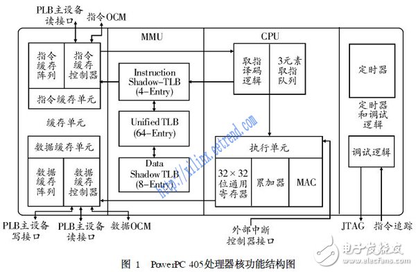
The CoreConnect bus architecture is an on-chip bus communication connection technology developed by IBM. The CoreConnect bus includes a processor local bus (PLB), an on-chip peripheral bus (OPB), and a device control register bus (DCR). The PLB bus provides high-bandwidth, low-latency connections between the master and slave. The OPB bus provides a way to connect peripherals with different bus width and timing requirements, reducing the impact on PLB performance. Controls the transfer of data between the general purpose registers and device registers in the PowerPC405 processor.
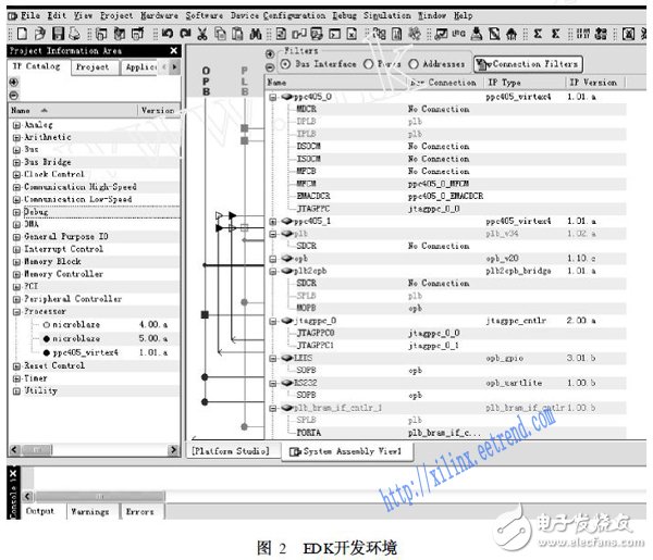
2 SoPC-based embedded system design technology 2. 1 platform technologyBuilding an embedded system based on the platform provides designers with great convenience. Xilinx's Embedded Development Kit (EDK) integrates such as hardware platform generator (platgen), hardware simulation model generator (SimGen), A series of tools such as software platform generator ( libgen), application software compilation tool (GNU Compiler), and software debugging tool (GNU Debugger). Designers can easily call a variety of tools for SoPC-based embedded system design through the Xilinx Platform Studio (XPS) integrated in the EDK environment. The EDK environment provides system designers with a wealth of IP resources, and can quickly build their own embedded systems using existing resources to complete the development of the entire PowerPC system hardware. If the IP library provided by the development kit does not meet the needs of the system designer, the designer can also customize his own IP. Figure 2 shows the graphical interface of the EDK development environment.
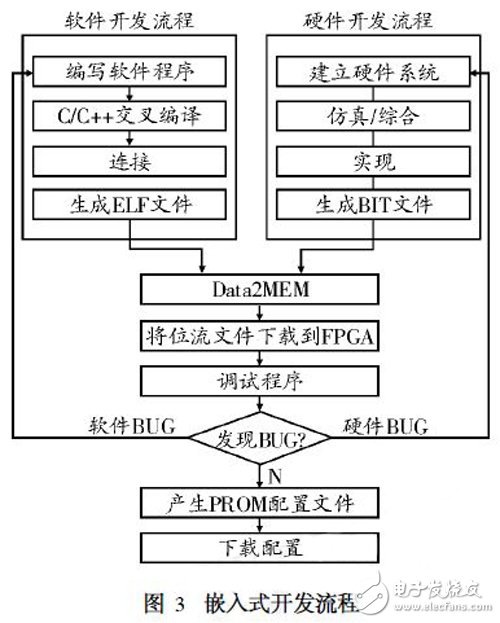
The EDK environment provides drivers and associated functions for its own IP, and designers can speed up application development by calling these functions. For the IP developed by the designer, you need to write the corresponding driver. After the application is written, call the GNU tool under EDK, compile the connection to generate the executable file, and then combine the hardware and software files to generate a downloadable bit stream file to download to the FPGA, using the Xilinx microprocessor debugging tool (XMD). Connect the GNU debugging tool for application debugging. After confirming that the application is correct and can implement the system function, you can convert the bit stream file into the PROM configuration file (MCS file) and download it to the PROM on the target board to complete the whole. Design and Development. Figure 3 shows the flow of embedded system development using EDK tools.
In the SoPC-based embedded system design process, the system designer must first clarify the design requirements, which has a guiding role for the entire design, and is also one of the standards for verifying the design availability after the design is completed. The system designer determines its system architecture according to the design requirements, defines the main module components of the system, determines its interface type, bus structure, hardware functions and software functions. The complete system architecture definition must meet the basic design requirements and maximize the Improve overall system performance.
Pvc Junction Box,Cable Junction Box,Plastic Junction Box,Electrical Junction Box
FOSHAN SHUNDE LANGLI HARDWARE ELECTRICAL CO.LTD , https://www.langliplastic.com