As shown in the figure, the resistor R and the photo-electric element LR and the potentiometers W1 and W2 constitute a voltage dividing circuit. When there is no light at night, the resistance value of LR is higher, and the voltage drop above it is larger, so the base current input to the transistor VT1 is larger, VT1 is turned on, and VT2 is also turned on, and the base current is turned on. After VT1 and VT2 are amplified, a part of the collector output of VT2 is coupled to the base of VT1 via capacitor C to form a positive feedback, which satisfies the oscillation condition of the circuit. Since the capacity of C is large, the oscillation frequency is very low, and VT2 supplies the amplified oscillation signal to the signal lamp ZD in the form of a pulse current, and it emits light by flashing. When there is light LR in the daytime, the LR internal resistance drops. Therefore, the base current flowing into the VT1 through R is greatly reduced due to the shunt, so that VT1 is turned off from conduction, and VT2 is also turned off, and ZD is extinguished. At this time, the silicon photovoltaic cell generates a higher voltage due to light irradiation and charges the battery. Adjust R and C to change the flash frequency and the time between light and off. Since W1 is connected in parallel with W2 in parallel with LR, adjusting the resistance of potentiometers W1 and W2 can change the voltage Veb between the base and emitter of VT1. Generally, the silicon tube is at Veb ≥ 0.6V~0.7V. When it is turned on; if it is turned off, the lamp can be ignited or extinguished as needed.
Component selection: Solar cells can be selected from 2CR or 2DR silicon photocells. LR can choose domestic 625-A type cadmium sulfide photoresistor. The photoresistor has a resistance value less than 50kΩ when there is light, and the resistance value is greater than 50MΩ when there is no light. The diode VD prevents the battery current from flowing back to the solar cell when there is no light or the light is weak (the voltage of the solar cell is lower than the battery voltage). Generally, the maximum operating current of the VD is greater than the maximum output current of the solar battery pack, and the reverse withstand voltage is higher than the battery voltage. If you use the c and b poles of the 3AX31 or 3AX81 low frequency tube, it is easy to meet the requirements. R is determined during the adjustment, and a small (1/8) W fixed resistor of about 47 kΩ is generally selected. The ZD is a small incandescent lamp of 2.5V and 0.3A. Other components are shown in the figure. 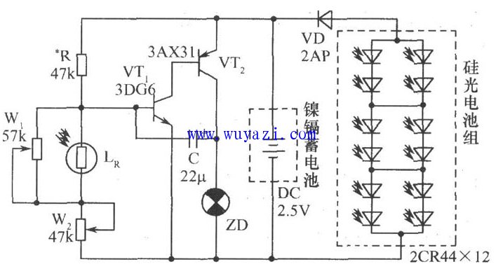
About this item
Strong Steel Material: The mining rig frame made of highest quality steel, with the finest craftsmanship, which is easy to install and has a sturdy structure. Keeps the machine perfectly organized while it holds the least amount of heat possible.
8 GPU Ports: The mining machine system comes with 8 GPU interfaces. Support ATX Motherboard, built-in, external dual PSU hosting, PSU mounting, hard drive. 8 GPUs can be installed on the motherboard at the same time. It supports RTX 3060TI 3070 3080 3090 6800/6800XT 6900/6900XT etc (Except 3060, because 3060 GPU need dedicated motherboard).
Generous Space between GPUs: The Gap between GPU ports is about 65mm, it can ensure low power consumption, reduce heat generation, energy-saving, and safe use.
Great Cooling Fans: The mining rig case is equipped with 4X120mm 3000 rpm high flow cooling fans, accelerating the air convection, enhancing the cooling and extending the service life of graphics cards.
gpu miner,best gpu mining rig,graphics card mining rig,ethereum mining,eth mining
Easy Electronic Technology Co.,Ltd , https://www.yxpcelectronicgroups.com