The charge pump works by first storing energy and then releasing the energy in a controlled manner to obtain the desired output voltage. Switching regulator booster pumps use inductors to store energy, while capacitive charge pumps use capacitors to store energy. The capacitive charge pump implements voltage boosting through a switch array and oscillator, logic, and comparison controllers, and uses capacitors to store energy. Due to the higher frequency, small ceramic capacitors (1μF) can be used, which minimizes space and costs. The charge pump converter does not use an inductor, so its radiated EMI is negligible. The input noise can be filtered out with a small capacitor. Charge pumps are ideal for portable applications such as cellular phones, pagers, Bluetooth systems and portable electronic devices.
1. Analysis and design of working principle of charge pump circuitA charge pump, also known as a switched-capacitor voltage converter, is a DC-DC that uses a so-called "flying" or "pumping" capacitor instead of an inductor or transformer to store energy. They can raise or lower the input voltage and can also be used to generate a negative voltage. The internal FET switch array controls the charging and discharging of the flying capacitor in a manner that doubles or reduces the input voltage by a factor (0.5, 2 or 3) to achieve the desired output voltage. This special modulation process guarantees an efficiency of up to 80% and requires only external ceramic capacitors. Since the circuit is switched, the charge pump structure also produces some output ripple and EMI (electromagnetic interference).
The charge pump maintains a stable output voltage by controlling the pump capacitance and regulating the switch. The charge pump switching network can achieve parallel or serial arrangement of pump capacitance during the pump capacitor charging and discharging transition cycle. Under the given input and output conditions (differential voltage), the optimal operating mode of the charge pump should be selected to maintain the required output voltage. The MOSFET device used in the charge pump switching network has the characteristics of small size, low cost, fast switching speed and lowest loss.
2, charge pump circuit research and design 2.1, compare boost circuitSince the design uses Vcom to be a constant voltage and the M2 tube gate pulse signal driving circuit works, it is required that the excitation signal should be based on the center potential, and alternately output low level and high level signals to realize periodic supersaturation of the probe. State, this design uses 0V as the ground potential and 5V as the high potential, so the comparator circuit is used for boosting.
The circuit is shown in Figure 1. The pulse signal is connected to one end of the comparator and the other end is connected to a DC level of 2.5V for comparison. When 0V is input low, the comparator outputs a high voltage of 5V, and vice versa, it outputs a 0V ground voltage. The comparator is connected to a 5V DC voltage at a high level and is grounded at a low level. The booster circuit also requires a large slew rate on the basis of the logic function to increase the conversion speed of the high and low levels. Transistors M10~M13 form a two-stage inverter to increase the slew rate of the circuit.
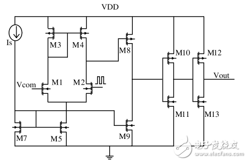
Figure 1 comparator boost circuit
The circuit diagram consists of three parts: a primary operational amplifier circuit, a secondary operational amplifier circuit, and a bias circuit.
This circuit diagram consists of 7 pmos and 6 nmos tubes, of which M1~M5 constitute a first-level operation, M7~M8 constitute a second-level operation, an amplifying circuit, and an M10~M13 two-group inverter. M5 and M9 have a common source and gate, resulting in the sum of their current magnitudes proportional to the width-to-length ratio of M7. M10~M13 function: Since the output of the secondary operational amplifier is an analog signal, it changes between Vmin and Vmax, and the inverter composed of M10 and M11 makes the intermediate value of the output more accurate. The inverter consisting of M12 and M13 makes the conversion more obvious and in place. At the same time, the transistors M10~M13 form a two-stage inverter to increase the slew rate of the circuit.
Design parameter calculation is a key step in the design of this circuit diagram. The current source of this circuit diagram is IS=400μA, Vdd=5V, Vcom=1.4V, and the M2 input is a step signal, Vmax=2.5V, Vmin=1V. M7 is connected in series with the current source, so the current through M7 is also IS, the gate of M5 is connected to the gate of M7, and the sources of M7 and M5 are both grounded, so the current through M5 is also IS. In the first-stage amplifier circuit, M1, M3 and M2, M4 are connected in parallel, so the current through M1 and M3 is equal to the current through M2 and M4, and is equal to IS/2; one group of M10 and M11, one group of M12 and M13, as long as The circuit function can be realized in accordance with the inverter circuit design.
2.2, bandgap reference voltage source design ideas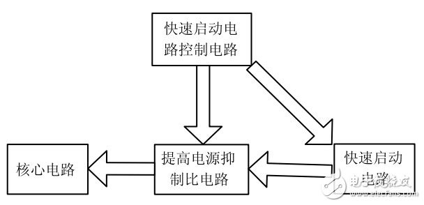
Figure 2 is the equivalent structure of the circuit
In order to improve the rejection ratio of the reference source at high frequency, the circuit adds an RC filter at the output of the reference source. Considering that the capacitor will prolong the startup time of the circuit, a fast start circuit and a fast start circuit for charging and discharging the capacitor are added to the circuit. The control circuit, once the startup is completed, the fast start circuit control circuit turns off the fast start circuit. The equivalent structure of the circuit is shown in Figure 2. In the circuit, the control circuit of the fast start circuit is a judging circuit for detecting whether the voltage at the output end of the reference source reaches a stable value, and also functions as a temperature compensation, so that the output of the reference source is provided without increasing the complexity of the circuit. Very good temperature characteristics. The actual circuit diagram of the bandgap reference is shown in Figure 3.
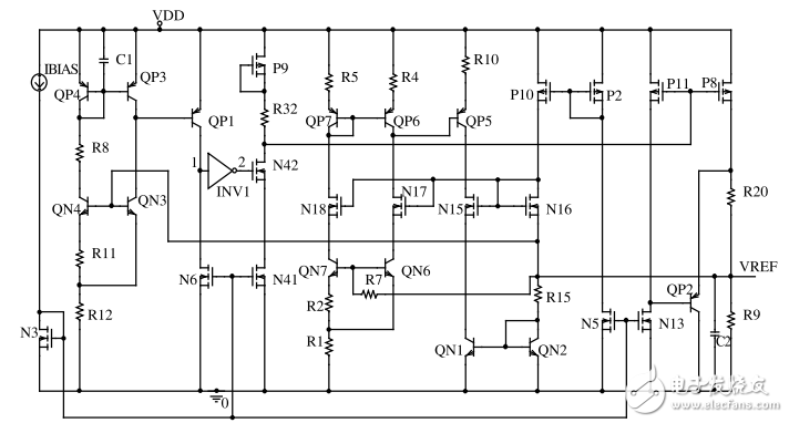
Figure 3 band gap reference source actual circuit diagram
2.2.2, the core circuit
The core circuit of the bandgap reference actual circuit diagram is to use a two-tube bandgap reference voltage source, which is the core of the design of the bandgap reference voltage source circuit, and is an essential step for the next step of design, as shown in Figure 4.
In Fig. 4, the emitter areas of the two tubes QN6 and QN7 are not equal, QN7 is larger than QN6, and the ratio is 8:1, and their bases are connected together. QN6 and QN7 respectively have mirror current sources composed of QP7 and QP6 as collector active loads, and the collector currents of the two tubes are equal.
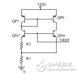
Figure 4 core circuit
Onlyrelx Bar2000 dual flavor is portable and fashion disposable electronic cigarette, disposable ecigs pen are trending featured vape pen for vapors as it's safety and easy to use. Disposable vape pod,disposable vape, wholesale vape,vape wholesale,vape pen manufacturer and supplier.disposable vape pen,disposable electronic cigarette,disposable ecigs pen,disposable ecigs stick,disposable e-cigs pen,disposable vape factory,disposable vape pod,disposable vape device,vape pen,vape stick, vape wholesale,wholesale vape,customized dispsoable vape pen,customized vape pen,OEM&ODM disposable ecigs pen,disposable electronic cigarette wholesale, wholesale disposable electronic cigarette,distribute vape pen,vape pen distribute,high quality vape pen,high quality vape pod,rechargeable disposable vape pen,refillable vape pen,refilling electronic cigarette,rechargeable disposable electronic cigarette,refillable vape pod,disposable refillable ecigs,disposable refilling e-cigs pen,refillable e-cigs pen
Onlyrelx Bar2000 Dual Flavor,Disposable Vape Pen E-Cigarette,Disposable Vaporizer E-Cigarette,Best Electronic Cigarette Vape Pen
Shenzhen Onlyrelx Technology Co.,Ltd , https://www.onlyrelxtech.com