The rapid development of electronics and its manufacturing technology has enabled the rapid adoption of Micro-Electro-Mechanical-SySTems (MEMS). In fact, MEMS-based accelerometers, pressure sensors, gyroscopes, etc. have been used for more than 30 years, but due to various reasons such as technology and cost, these technologies are mainly used in industrial, military, automotive, instrumentation, and medical. And other fields, but not into the consumer products market. The current situation has changed dramatically. MEMS technology is not as expensive as jewelry a few decades ago. Low-cost, small-size, low-power, high-performance MEMS sensor products have set off a new wave of design and consumption.
Multi-axis accelerometers based on MEMS technology are currently mainly used in gaming machines and mobile phones, hard disk anti-drop protection, fitness step measurement of portable devices, and anti-shake of digital cameras/cameras. In addition, physical sensors for measuring physical quantities such as thermal effects, light intensity and pressure are also among the future priorities.
ST has been committed to the widespread use of MEMS technology and the investment in the development of new products and technologies. It is the first to invest in an advanced eight-inch wafer production line while promoting complementary partnerships. ST's goal is the popularity and mass production of MEMS products in the consumer field, which has become the driving force of the technology consumer wave.
1. MEMS Overview
Microelectromechanical systems refer to three-dimensional mechatronic structures fabricated by silicon wafer micromachining technology, which began to appear in semiconductor factories in the 1960s. Physical sensors of MEMS technology are often seen in people's daily lives to sense acceleration, angular velocity, pressure and sound pressure.
Automotive electronics is a rapidly growing market, and MEMS technology is everywhere. Acceleration or Yaw Rate sensors are used to protect the safety of passengers in all active and passive safety systems such as automotive dynamics control and airbags. To reduce fuel consumption, pressure sensors are also used in engine manifolds. Manifolds) and Fuel Lines.
MEMS technology has set off a climax of product design innovation in the active consumer electronics market. For the consumer market, MEMS products are often the best solution for technical and economic considerations, and provide a blueprint for miniaturization and advanced levels of future development. One of the most successful applications is the new control experience that accelerometers bring in Nintendo's Wii and Sony's PS3 consoles. In the past, accelerometers were only used in active and passive safety systems in automobiles, and some safety regulations required one of the driving forces for their application in automotive electronics. Today, “sensing and simplification†has become the value proposition of MEMS in the consumer product market. It is also the dream of design master Naoto Fukusawa-san to remove all the barriers between the complex world of users and electronic devices. In addition, the three-axis accelerometer can also be used to design hard disk drop devices to protect data security; the UI control of portable devices can also be used to achieve more user-friendly functions.
MEMS components are identical to CMOS in chips and are manufactured using semiconductor fabs. But the difference is that MEMS components are not just electronic products, but also incorporate many mechanical structures, such as movable mechanisms such as Spring, Electrode, Membrane, and CanTIlever. . In addition, silicon micromachined components often compete with the price, size, and performance of traditional quartz or piezoelectric products.
Motion sensors such as accelerometers and gyroscopes bring motion detection capabilities to silicon components. The application of such components in the automotive market will continue to increase, and the requirements of some bills are one of the driving forces; the application in the consumer market will also be greatly improved, and its growth rate will be very fast. Multi-axis accelerometers have only been used in active and passive safety systems in automobiles, but are now more widely used in notebooks, hard drives, cell phones and game controllers. In addition to automotive dynamics control systems, offset rate sensors (gyros) are also used to improve image stability for digital cameras and cameras. In addition, motion sensors and magnetometers are expected to be integrated into motion measurement units to provide personalized navigation for handheld devices, enabling the implementation of location-based services (LBS) from telecom operators.
The industry predicts that motion sensors such as accelerometers and gyroscopes will continue to increase in the consumer electronics market and grow rapidly.
Multi-axis accelerometers provide motion detection for silicon components and are currently used in hard drives, handheld devices, notebook computers, cell phones, game consoles and more. Gyroscopes are also used in digital cameras and camcorders to support their anti-shake function. In addition, motion sensors and magnetometers are expected to be integrated into motion sensing units to provide personalized navigation for handheld devices, providing a platform for telecom operators to provide location-based services (LBS).
Micro-pressure sensors have been used in a large number of vehicles, mainly in the detection of tire pressure; in addition, medical equipment is also one of its main markets. With the advancement of technology, the development cost is gradually reduced and the size is thinner and lighter. The miniature pressure sensor is expected to be accepted by the consumer market very quickly and used in new fields such as wireless communication.
Due to size limitations of mobile phones and notebooks, the use of conventional electret condenser microphones using surface mount technology (SMT) is limited, so MEMS-based capacitive silicon crystal microphones will rapidly spread in this market.
The integration of various components such as accelerometers, gyroscopes, and pressure sensors will be an inevitable trend in the future. MEMS product suppliers need to develop a common technology platform that integrates multiple sensors based on customer needs. THELMA and VENSENS are two technology platforms for sensor integration. ST's MEMS product manufacturing and R&D are carried out in advanced 8-inch MEMS fabs, enabling shorter time-to-market and quickly meeting market demands. In addition, the company is actively developing multi-axis gyroscopes, pressure sensors and capacitive silicon crystals, and is actively working with other companies to launch sensor products with market potential or customer requirements.
2. Physical processing micromachining technology
Silicon crystals have become the most popular material in MEMS manufacturing due to their excellent electrical, mechanical and thermal properties. MEMS sensors are typically fabricated and fabricated by the same so-called Micro-Machining process technology as the chip's basic process technology. However, other materials such as quartz, glass, plastic, and ceramics can also be used for micromachining or microforming. For example, quartz and ceramics are often used in crystal oscillators (CrySTal Resonator) and Kodak force gyroscopes.
In addition to its superior physical properties, silicon crystals are another reason for their industrial structure considerations. The global microelectronics industry has invested huge sums of money and accumulated a lot of professional experience to build a solid industrial infrastructure. Manufacturers can use the proven manufacturing technology developed for silicon chip production to produce MEMS components and simultaneously produce thousands of micromachined components using silicon wafers. The huge economic scale used to be an important condition for the success of the electronics industry. Now MEMS can replicate successful technologies and experiences in this way to design and mass-produce silicon microelectronic components, while also working on transistor size. Further narrowing down. In addition, the wafer fabrication process is managed by extremely rigorous procedures and processes, so design repeatability and production yield are higher compared to other process approaches.
The physical properties of silicon are very strange. Its material is brittle, but it is not easy to produce plastic deformation; it can make steel harder, but it weighs only one-third. Due to these characteristics of the material, after it is integrated with the integrated circuit, the electrical quantity generated by the moving structure such as the diaphragm or the cantilever arm in the MEMS mechanism can provide the measured physical quantity or control capability of the sensor.
The main reasons for the widespread use of MEMS are their extremely small size, high reliability and low power consumption, enabling faster and more accurate operation than other larger competitors. On the other hand, for ordinary users, especially in the field of price-driven consumption, cost considerations cannot be ignored.
At present, the size of MEMS components is also micron-sized, which can be manufactured by the earlier 6-inch fab. However, with the rapid growth of demand for related applications in the consumer market and price pressure, many manufacturers are expected in the next few years. It will be moved to the 8-inch production line. ST has already realized the shift to the 8-inch production line, and the excellent competitive advantage in both technology and cost has made the company take the initiative in the market.
Many micromachining processes are currently derived from basic IC fabrication techniques such as Photolithography, Material DeposiTIon, ReacTIve Ion, and Chemical Etching. Although more and more components are currently being manufactured into CMOS processes, due to different situations, different considerations are still needed for different applications.
For example, the MEMS component micromachining scale is between tens and hundreds of micrometers, and there is still a gap between the chip circuit; therefore, wet etching, generation or plating of thin films, wafer stacking, vias (vias), and dry etching are Common micromachining manufacturing procedures today. In particular, MEMS components will also use materials such as gold or glass media, which are completely prohibited in CMOS processes.
In order to achieve differentiated competitive advantages, MEMS suppliers have developed proprietary micromachining process technologies suitable for their products in recent decades based on their own and equipment characteristics, as well as the process steps they are good at.
The proprietary processes of each manufacturer can be broadly divided into two categories: bulk micromachining and surface micromachining. Body micromachining is a "subtraction process" by removing the substrate to form the desired structure. Suitable for designing thicker structures, the designer can freely determine the required substrate thickness, but the shape of the micromachined structure is limited by the crystallographic configuration of the silicon substrate. The opposite surface micromachining is an “addition processâ€. The main process is to remove or leave individual regions of different material layers through different processes according to specific needs, and the substrate layer remains intact. Because the thickness of the material layer film (Film) can be generated or deposited on the substrate is limited, the technology is limited to thin components of about 2 microns, but the new wafer bonding technology (Wafer Bonding) technology helps to design thicker element. With these lithographic techniques, mechanical structures that are otherwise very complex and highly innovative can also be made relatively simple.
3. THELMA and VENSENS micromachining processes
ST's current micromachining process for mass production is available in THELMA and VENSENSE, both of which are hybrid manufacturing technologies for bulk and surface micromachining technologies.
THELMA is known as the Thick Epitaxial Layer for Microgyroscopes and Accelerometers and is mainly used for high-performance and low-cost motion sensors such as accelerometers, gyroscopes and microphones. The THELMA process begins with a standard silicon wafer with a first layer on it as an isolated oxide layer (about 2 microns). A layer of interconnected polysilicon is then deposited, and a second sacrificial oxide layer (about 2 microns); in this layer, it is responsible for the support point of the fixing mechanism and the individual points of the fixed end of the moving mechanism. Etching is performed to create holes. A thicker layer of germanium (about 15 microns) is then formed on it, and this layer is etched with a mask to create a structure that combines both moving and fixed cells. Finally, the sacrificial oxide layer underneath this structure is removed by isotropic etching to shape the mobile unit. To reduce or eliminate the effects of humidity or air density variability, which in turn affects the resonant frequency of the component, the open space near the structure is filled with air, typically dry nitrogen. The second wafer is then bonded to the first sheet to protect the tiny mechanism from damage under high pressure applied during the InjecTIon Molding program.
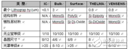
Table 1 Comparison of CMOS, Body, Surface, THELMA, VENSENS Micromachining Processes
VENSENSE is the abbreviation of Venice Process for Sensor, which can realize a very compact pressure sensor. It also starts with a standard silicon wafer, and the results are quite similar to those of a wafer bonding process using bulk micromachining. A dedicated dry and wet silicon etch mixing step can produce a single crystal silicon layer and form on it. A layer of sacrificial layer less than 3 microns thick, the thickness of the structural layer can reach 20 microns. However, compared with bulk micromachining, VENSENSE can produce thinner, smaller and more stable mechanical properties of the chip; in addition, the tight bonding of the pores does not require any wafer-to-wafer bonding, so the reliability of the tight connection higher.
Due to the excellent electronic properties of single crystal silicon, stable and reliable resistors can be integrated into the structural layer by processes such as implantation or diffusion. These resistors are then connected to an aluminum metal layer to implement the four branches of the WheatSTone Bridge. This metal layer is then covered by a standard insulator such as Silicon-Oxynitrid or the like to provide protection against external corrosive agents. Because the bridge has excellent monocrystalline silicon lamination resistance, it is quite sensitive to pressure changes.
4. Motion sensors in the consumer electronics market
The consumer electronics market has its own characteristics, and consumer products need to achieve low prices, low power consumption, low voltage, and miniaturization. MEMS product suppliers must increase the speed of development of new products while maintaining the same reliability as automotive electronics.
Accelerometer gyroscopes have been widely used in the automotive and medical device markets, such as automotive active or passive safety systems and heart rate adjusters. The consumer market is manufactured differently than the large, thick and expensive ceramics used in the automotive electronics market. It prefers surface mount packaging and small, thin and low cost solutions. For example, ST's Full Molded PLGA, which was released in 2002, is now widely used in the industry as a process standard. With this technology, it took ST less than three years to miniaturize its 3-axis accelerometer series from 100 cubic millimeters to 10 cubic millimeters.
Automotive sensors are not powered by batteries, so power consumption is not a technical difficulty, and high seismic performance is important. In addition, a wider temperature range and higher product credibility are also basic requirements in the automotive product market. For the consumer market, power consumption and voltage are one of the priorities. The current supply voltage for consumer products has dropped to 1.8 V and the current must be less than 1.0 mA.
Because the handheld device does not have a fixed frame as a reference, and the user wants the motion in all directions to be detected by the acceleration sensor and realize the corresponding function, the current multi-axis sensor solution is the mainstream of the consumer market.
Sensor solutions for analog outputs are also being replaced by digital products because digital solutions make product integration easier and software development faster. In addition, increasing the pin position of the interrupt function simplifies the integration of the final product and is one of the customer's needs. In response to these demands, ST has developed two-axis, three-axis, analog and digital accelerometers to suit different applications. ST also offers reference design and evaluation kits, as well as dedicated development software tools.
Monolithic and two-chip single-package hybrids (Hybrid) in a single-chip single package are the two main solutions on the market. The multi-chip, single-package solution is not only cost-effective, but also provides the modularity and flexibility required for rapid mass production, which is important in the consumer market. However, due to the requirements of the actual system in terms of cost, time to market, etc., it is wise to adopt the most appropriate solution. It is feasible to integrate the sensing unit and the interface circuit at present, but it is not necessarily the best solution. Sometimes using standard CMOS technology to create complex control circuits can better meet both functional and cost requirements.
ST's accelerometers and gyroscopes feature a system-in-package (SiP) solution in a single package of two chips. One of the two chips is manufactured by THELMA micromachining technology and is sensitive to inertia or Kodak force; the other can be an analog or digital control chip that is mechanically processed with THELMA side by side or stacked. The components are packaged together.
In the SiP architecture, the micromachined sensor chip converts the acceleration into a differential capacitance change, and the other interface chip converts the tiny capacitance change (atto-farad range) into an analog or digital format output signal.
The SiP method accelerates the development of new motion sensors such as multi-axis gyroscopes. Thanks to the modular design of the LEGO toy, the mechanical and electronic modules of the gyroscope can be used in the same technical platform as the mass-produced multi-axis accelerometer. The designer can verify the multi-axis accelerometer. Function modules are re-used to speed up development and achieve lower development costs. In addition, thanks to the flexibility of the Land Grid Array package configuration, ST can quickly integrate any two modules in its chip into the final product, even including pin adjustment.
5. Pressure sensors in the consumer electronics market
The traditional application of pressure sensors is the measurement of physical quantities such as pressure and air flow, mainly in industrial, automotive and medical applications. MEMS-based pressure sensors can be used to measure physical values ​​such as resistance or capacitance changes. The processing and manufacturing mainly adopts the body shape processing or the surface type processing mentioned above, or a mixture of the two. The pressure sensor material is typically a silicon semiconductor, and a standard silicon substrate or a more expensive silicon-on-insulator (SOI) substrate is also used as the starting layer material.
Pressure sensors can be divided into resistive and capacitive types, and correspond to different processing processes. Body micromachining technology is the better choice for resistive pressure sensors; capacitive pressure sensors are generally more suitable for surface micromachining.
The resistive working principle utilizes the piezoresistive properties of silicon crystals to convert tiny diaphragm stresses into tiny resistance variable variables. Capacitive pressure sensors use two parallel plates, one fixed and the other perpendicular to the chip. A thin diaphragm that moves in the direction of the plane. When there is movement, there is a very small change in capacitance between the two boards and an output is produced. The output resistance or voltage value is transferred to the interface circuit and converted to a voltage value. As with motion sensors, interface circuits can be integrated in either chip or package form. The SiP structure provides greater design flexibility and speeds time to market.
The manufacturer's customized process is currently the mainstream of MEMS micromachining technology, and there is no so-called ideal process. But no matter how many different semiconductor fabs and processes exist on the market, the key to consumer products is always the trade-off between price, size and performance. This situation has caused only a few vendors to provide viable solutions for the consumer market. For example, in standard body-type micromachining solutions, the package part is often the main part of the cost, and the VENSENS technology can produce a low-cost miniaturized silicon crystal with a size of only 0.8mm x 0.8 mm and a thickness of about 0.3 mm. (Full Silicon) pressure sensors have the advantage of making performance independent of the packaging approach, clearing the barriers to entry into cost-driven consumer products. ST's recently released patented HLGA (Holed Land Grid Array) technology enables its pressure sensor's Re-Use motion sensor to have both production tools that enable consumers to get smaller and thinner packages.
6. Types of consumer applications for motion and pressure sensors
15W Wall-Mounted Power Adapter
15W Wall-Mounted Power Adapter,24V0.5A Ac Dc Power Adapter,5V2A Power Adapter,5V2.5A Clear Enclousure Wall Charger
Guangdong Mingxin Power Technologies Co.,Ltd. , https://www.mxpowersupply.com