For more than forty years, MEMS oscillators have only recently become commercially available, and one of the biggest obstacles is the development of an economical and purely sealed packaging system. MEMS oscillators must be sealed in a very clean environment because even small surface contaminants can significantly change the oscillation frequency. In addition, because the package is cost sensitive, the package must also be low cost.
Therefore, MEMS oscillator packaging must meet four major requirements: (1) to provide an extremely clean internal environment; (2) to provide a stable mechanical structure; (3) miniaturization, suitable for CMOS integration and can take advantage of MEMS; (4) )low cost.
SiTIme's MEMS-First wafer level containment and packaging technology meets these requirements. SiTIme's MEMS oscillators are hermetically sealed by embedding epitaxial layers of polysilicon under the surface of the wafer and, along with the driver circuit, are diced and cast into standard plastic package integrated circuits. This hermetic and packaging technology is inexpensive and very clean. Silicon MEMS oscillators fabricated using this technology have similar performance to quartz oscillators and are expected to be used in large-scale commercial applications.
Pay special attention to the package cleanliness of the reference oscillator. The unpackaged oscillator can drift by up to hundreds of ppm per day. Quartz oscillators in the dominant time reference source market are typically packaged in metal or vacuum ceramics, and similar packages can be used for MEMS oscillators, but have stability issues. Anodized bonded overlay technology provides a clean environment for oscillator types in certain applications, but still does not provide adequate cleanliness and is not universal.
MEMS oscillator packages should take advantage of the advantages of MEMS, that is, small size, integration with CMOS processes, and cost reductions from integrated circuit fabrication techniques. Otherwise, MEMS oscillators are hard to compete with mature quartz technology.
When MEMS require durable coverage, typical solutions include wafer bonding of large micromachined silicon or glass-covered wafers. Wafer bonding technologies are already in volume production, for example they have been used in Bosch's airbag and yaw sensor applications. Wafer bonding technologies include, for example, glass melting, soldering, compression bonding, and the like.
Although this coverage requires mechanical protection, it provides a sufficiently clean environment for the clock reference IC in only a few special cases. Binding coverage leads to a significant increase in system cost, often exceeding the cost of the oscillator itself. They require assembly and wafer-to-wafer overlay alignment, doubling the thickness of the MEMS device, and requiring a large chip area for the placement of the closed loop and bond pads. Closed-loop and bonded pads can occupy 80%~90% of the chip area, and the cost accounts for 80%~90% of the cost of the packaged MEMS oscillator.
Thin film packaging technology is an alternative to bonding coverage, typically based on thin film layers such as low pressure chemical vapor deposition (LPCVD) nitrides or polycrystals, or based on gold plated metals. This technique does not have a large seal ring and is not limited by the binding layout, but generally does not withstand the pressure of injection molding and does not provide sufficient cleanliness for the frequency reference source. SiTIme's sealing technology is based on epitaxial polycrystals and is sealed by an oxide that is designed to withstand accelerated environmental applications rather than being optimized for clean environments.
The test results for the oxide hermetic package show that the resonator has a frequency hysteresis of tens of ppm when the temperature changes. Epitaxially sealed resonators have been successfully applied to resonant pressure sensors, which are packaged in a pure single crystal process electrochemical structure.
SiTIme's seals do not require seals or tight bond pads, and electrical connections can be routed to any suitable location on the chip surface for more efficient use of chip area (chip area is only one-tenth the size of the bond overlay technology) . This seal has a high mechanical strength and can withstand hundreds of atmospheres while changing the chip package injection molding process. This seal also provides a very pure and stable vacuum environment, making it ideal for reference oscillator applications. The sealed MEMS oscillator stability data presented here is similar to a quartz crystal oscillator. Finally, it is worth mentioning that the product process is very economical and can greatly save costs.
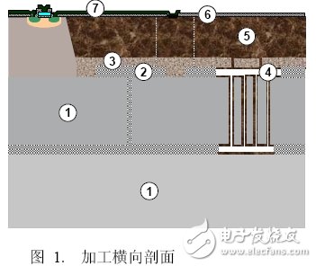
Processing technologyThe fabrication process of the SiTime resonator is shown in Figure 1: (1) forming a resonator structure pattern by reactive ion etching (DRIE) on a 10-20 um thick SOI (insulator silicon) substrate; (2) depositing a layer of oxide And patterning to cover the selected resonator portion and providing electrical contact to the drive and sense electrodes; (3) depositing a 1.5 um thick epitaxial layer and forming a pad to the oxide; (4) The hole excavates the oxide above and below the free space of the resonator structure; (5) the cavity is sealed in the epitaxial environment by SiTime's EpiSeal process to form a clean sealed space; (6) the wafer is planarized by chemical mechanical polishing (CMP), and the insulation is formed. The contact pattern is extended to be bent into a 10-20 um thick epitaxial polycrystalline sealing layer; (7) deposited to form an insulating oxide layer, a metal connection and a mask, or a CMOS.
After the oxide is removed, the first and second depositions are deposited on the oxide layer and the single crystal to grow polysilicon, which is integrated into the CMOS circuit by exposing the CMP to a single crystal smooth region. The circular cavity has a vacuum of up to 10 mT, which essentially prevents water pollution and high pressure pollution.
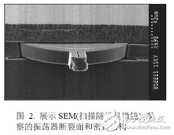
Figure 2 is a complete scanning tunneling microscope (SEM) structure diagram of the process prior to contact and metallization, from which the wafer surface and cross-sectional structure of the package and resonator can be seen.
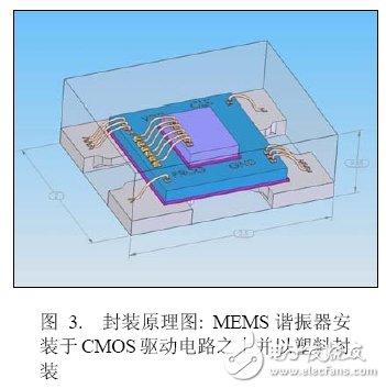
The sealed resonator is diced and packaged in a standard injection mold. Figure 3 shows the design principle of a 2.5 x 2.0 x 0.85 mm plastic package, which is to mount the MEMS resonator on top of the CMOS driver circuit. This packaging method is cost effective and is a compromise for QFN/MLF technology. It is a very small package in the oscillator and will be smaller in the future.
Measurements show that MEMS oscillators in this package are comparable to quartz oscillators in terms of initial frequency stability, long-term frequency stability, long-term package sealing performance, temperature resistance, and cycle temperature stability.
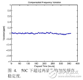
Figure 4 shows the initial frequency stability test data for a temperature-compensated MEMS oscillator. These data were collected after a few minutes of shaking at 50 ° C and the results showed an oscillation drift of less than 50 ppm over 14 days. Figure 5 is a long-term frequency stability data for an oscillator operating at 25 ° C for 8,000 hours. The total drift measured is 2 ppm within the 3 ppm range defined by the measuring instrument.

Figure 6 shows the frequency stability of the two oscillators during the temperature cycling test. The data was obtained at a positive temperature cycle of -50 ° C to +80 ° C and a temperature of 30 ° C in a negative temperature cycle. The data was collected from 600 temperature cycles with no frequency drift with a tolerance of 3 ppm.
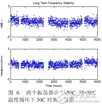
Figure 7 shows the compensated frequency stability data. The temperature is scanned twice from -40 ° C to +85 ° C and returned to -40 ° C. The total frequency error over the entire temperature range is less than 100 ppm (200 ppm measurement noise floor, 30 ppm measurement error) with a hysteresis of less than approximately 50 ppm.
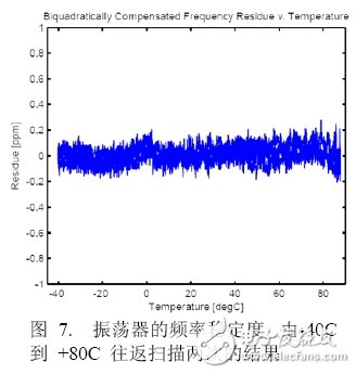
These results are comparable to the performance of a quartz oscillator. Due to the limitations of the instrument itself, the potential of resonance and packaging technology has not been fully realized. Measurements are done by high-performance laboratory instruments, reflecting the potential of the technology itself, rather than the scope of the product specification.
In summary, this article demonstrates a manufacturing process for MEMS oscillators and a set of measurement data comparable to traditional quartz crystal technology. These measurements are the most stable MEMS oscillator data available so far. This MEMS oscillator is suitable for commercial applications.
Solar Panel ,Flexible Solar Panels,Portable Solar Panels,Sunpower Solar Panels
zhejiang ttn electric co.,ltd , https://www.ttnpower.com