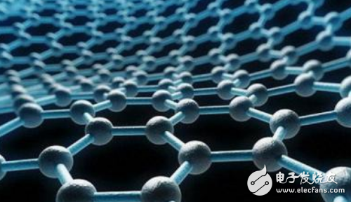
Graphene is a two-dimensional carbon nanomaterial composed of a carbon atom and a sp2 hybrid orbital to form a hexagonal honeycomb lattice. Graphene has excellent optical, electrical and mechanical properties, and has important application prospects in materials science, micro-nano processing, energy, biomedicine and drug delivery. It is considered to be a revolutionary material in the future. The physicist Andrew Gem and Konstantin Novoselov of the University of Manchester in the United Kingdom successfully separated graphene from graphite by micromechanical stripping, and jointly won the 2010 Nobel Prize in Physics. The common powder production methods for graphene are mechanical stripping method, redox method, SiC epitaxial growth method, and the film production method is chemical vapor deposition (CVD).
Graphene structureGraphene is a two-dimensional (2D) periodic honeycomb lattice structure composed of a carbon six-membered ring, which can be warped into zero-dimensional (0D) fullerene and rolled into one-dimensional (1D) carbon nanotubes. (carbon nano-tube, CNT) or stacked into three-dimensional (3D) graphite, so graphene is the basic unit of other graphite materials. The basic structural unit of graphene is the most stable benzene six-membered ring in organic materials, and is the most ideal two-dimensional nanomaterial.
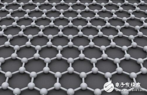
The ideal graphene structure is a planar hexagonal lattice, which can be regarded as a layer of stripped graphite molecules. Each carbon atom is sp2 hybridized and contributes to the remaining electrons in the p orbital to form a large π bond. The electrons can move freely, giving the graphene good conductivity. The two-dimensional graphene structure can be regarded as the basic building block for forming all sp2 hybrid carbonaceous materials.
The structure of graphene is very stable, and the carbon-carbon bond is only 1.42 Ã…. The connection between the carbon atoms inside the graphene is very flexible. When an external force is applied to the graphene, the carbon atom plane is bent and deformed, so that the carbon atoms do not have to be rearranged to adapt to an external force, thereby maintaining structural stability. This stable lattice structure gives graphene excellent thermal conductivity.
For the first time, scientists took a clear picture of a single molecule and saw the atomic bonds that bind the molecular structure together. A research laboratory at IBM International Business Machines (IBM) in Zurich, Switzerland, uses a technique called "non-contact atomic force microscopy" to explore the internals of a molecule, minimizing the study of molecules and atoms. This research may be important for the study of graphene devices.
At absolute zero, the valence band of the semiconductor is full (completely occupied by electrons). When exposed to photoelectric or thermal excitation, some of the electrons in the valence band (the electron velocity of graphene is as high as 105 m/s, which is 1/300 of the speed of light) crosses the forbidden band into the empty band with higher energy, and the electrons in the empty band become The conduction band, which lacks an electron in the valence band, forms a positively charged vacancy and becomes a hole. The electrons in the conduction band and the holes in the valence band are collectively referred to as electron-hole pairs, and electrons and holes can freely move to become free carriers. They generate directional motion under the action of an external electric field to form macroscopic currents, which become electron conduction and hole conduction, respectively.
Each unit cell of graphene has 2 carbon atoms, resulting in two equivalent conical intersection points (and K') points in each Brillouin zone. The energy near the intersection point is linear with respect to the wave vector.
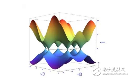
Graphene electron band structure diagram
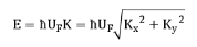
E: energy, h: reduced Planck constant, UF: Fermi velocity, 1*10^6m/s, Kx, Ky are the components of the wave vector and then the X- and Y-axis, respectively. Therefore, the effective mass of electrons and holes in graphene is made zero, and all electrons and holes are called Dirac fermions. The intersection point is the Qiulak point, the energy in the vicinity is zero, and the band gap (forbidden band) of the paleographene is zero. The unique carrier properties of graphene and the massless Dirac fermion properties allow it to observe Hall effect and anomalous semi-integer quantum Hall effect at room temperature (when the current is perpendicular to the external magnetic field through the conductor, the conductor A potential difference occurs between the two end faces perpendicular to the direction of the magnetic field and current. It shows its unique carrier characteristics and excellent electrical properties. The measured value of room temperature carrier mobility of graphene is 15000cm^2/·s (electron density 10^13cm^2).
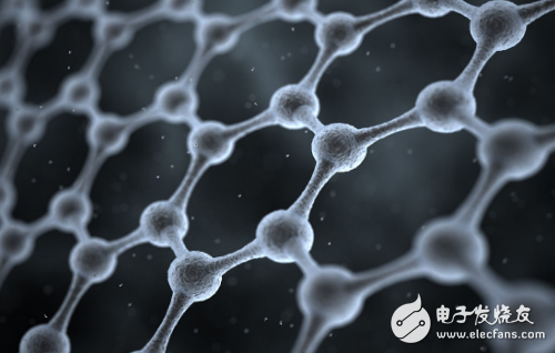
Lattice structure of grapheneThe lattice structure of graphene is very stable, and the interference of electrons moving in orbit is very small, and has excellent electrical conductivity. This structure results in a unique electronic band structure of graphene. The six vertices of the first Brillouin zone are Fermi points (also known as Dirac points or K points), and the conduction band and the valence band are symmetric about Dirac points. Therefore, in pure graphene, electrons and holes have the same properties. That is, near the Dirac point, the energy of the electron is linearly related to the wave vector, E = VFP = VFhk.
Among them, VF is the Fermi speed, which is about 1/300 of the speed of light, and k is the wave vector. Therefore, the electrons near the K point are affected by the surrounding symmetric lattice potential field, the effective static mass of the carrier is 0, and the Fermi velocity is close to the speed of light, exhibiting relativistic properties. Therefore, the electronic properties near the K point should be described by the Dirac equation, rather than by the Schrodinger equation. The mobility of graphene carriers exceeds 200,000 cm2*V-1*s-1, and the average free path of electrons in pure graphene is on the order of submicron, which is similar to ballistic transport, which is attractive in manufacturing high-speed devices. potential.
3 Phase Energy Power Meter With CTs For Solar Inverter
3 Phase Energy Power Meter With Cts For Solar Inverter,3 Phase Energy Power Meter Cts For Solar Inverter,3 Phase Energy Power Meter Cts Solar Inverter,Solar Inverter 3 Phase Energy Power Meter
TRANCHART Electrical and Machinery Co.,LTD , https://www.tranchart-electrical.com