At the beginning of 2017, SMIC, a leading semiconductor manufacturing company in China, officially used ReRAM (non-volatile resistive memory) chip with 40nm process, and Crossbar, the invention company of ReRAM storage technology, appeared in people. In the field of vision. In fact, when Crossbar entered the Chinese market in March 2016, it announced its cooperation with SMIC in the 40nm process. A year later, the official sample is enough to announce to the industry that ReRAM is really coming.
How important is the market for memory? Throughout the entire technology industry, storage space for future growth is still very large, 5G era, Internet of Things, artificial intelligence, the development of these technology products are inseparable from storage. Independent memory accounts for $95 billion in the market, and logic circuits that integrate with logic resistors and require embedded memory have a market size of 135 billion. In the Chinese market, the size of the memory is 20 billion, which has become a market that all major storage manufacturers are competing for.
Recently, "Electronic Technology Application" reporter interviewed Sylvain Dubois, vice president of strategic marketing and business development of Crossbar, and made some understanding and discussion on the latest development trend of ReRAM technology.

Sylvain Dubois, Vice President, Strategic Marketing and Business Development, Crossbar
Sylvain Dubois pointed out that Crossbar's memory technology will not only enter the $95 billion independent memory market, but also into the $135 billion market-scale logic. The Chinese market is a very important market for Crossbar.
Founded in 2010 and headquartered in Santa Clara, California, Crossbar is the industry leader in ReRAM technology, with 310 patents and 160 approvals. Sylvain Dubois pointed out that ReRAM technology can well fill the delay gap between DRAM and flash SSD: "Our strategy is to fill this gap. We have a very unique technology is the variable resistance of metal conductive filaments, It is resistive memory technology."
Potential for evolution to advanced process nodes such as 7nm
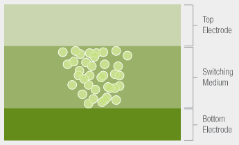
ReRAM three-tier architecture
ReRAM is a three-layer architecture based on a simple upper electrode, a resistive switching medium, and a lower electrode. The working mechanism of the resistive conversion medium is that when a voltage is applied between the two electrodes, conductive filaments are formed. There are different ways to implement ReRAM based on the different transformation materials and the organization of the storage unit. There are significant differences in device performance due to differences in conversion materials.
Crossbar's ReRAM technology uses a silicon-based conversion material as the host for the formation of metallic conductive filaments. When a voltage is applied between the two electrodes, nanoscale conductive filaments are formed. Because the mechanism of resistive switching is based on electric field, Crossbar's ReRAM memory cell is very stable, temperature can range from -40C to 125°C, more than 1 million write times, and data at 85°C. Save for 10 years.
Sylvain Dubois pointed out: "Our conductive filaments are very small and have a diameter of less than 5 nm. At the evolution of the process node, we are currently mass-produced at 40 nm. Because of its unique technology, it can be reduced to 7 nm. ReRAM is not like Flash, which can evolve to advanced process nodes, and can be stacked vertically in 3D, paving the way for terabytes of storage on a single chip."
Faster read and write performance than Flash Flash
Crossbar's ReRAM technology is based on a simple device structure that uses materials compatible with CMOS processes and standard CMOS process flows. It can be easily integrated and manufactured in existing CMOS fabs. Since the Crossbar ReRAM array is integrated in a low-temperature back-end process, a multi-layer Crossbar ReRAM array can be integrated on top of a CMOS logic wafer to build a 3D ReRAM memory chip.
Sylvain Dubois explained: "Because it is fully compatible with CMOS logic, it has a big advantage that it can be integrated into a CMOS GPU, can be produced in a CMOS logic foundry, or it can be produced in a memory foundry. It can be used as a Separate memory replaces the current popular NAND Flash, and there will be a large amount of NAND Flash in the SSD to implement the SSD function."
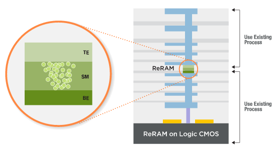
ReRAM integrated on CMOS logic wafers
Compared to traditional Flash flash, Crossbar ReRAM provides faster, bit-level flipping and no erase operations. It offers 100 times lower read latency, 1000x faster write performance than flash, and a smaller page architecture that reduces read and write latency, reduces power consumption, and increases the life of the memory solution.
Low cost, low energy consumption, high security
Nowadays, the artificial intelligence technology, which is very popular, uses deep architecture and deep neural network architecture to extract different features and realize feature recognition through matrix form, such as face recognition, speech recognition and pattern recognition.
Taking convolutional neural networks as an example, the convolution operation accounts for 90% to 99%. Different filters are needed to calculate and match the data of the input image. The matching output is 1, and the unmatched part outputs 0, so that Determine the mode of the image. There are a large number of models in the entire neural network that match different patterns.
The implementation of chips currently used for artificial intelligence requires very expensive on-chip SRAM, which can be done in CMOS circuits, but is expensive. With a small amount of SRAM and an external large-capacity DRAM on the chip, there are many memory access operations in the architecture using external DRAM and on-chip SRAM. The delay will be large and consume a lot of energy. Sylvain Dubois believes that Crossbar's technology can revolutionize the artificial intelligence chip.
"If you use embedded ReRAM to achieve, you can not need external DRAM to store a large amount of model data, the internal SRAM can also be minimized. Because the entire model parameters will be placed in ReRAM, ReRAM data directly participate in the calculation, ReRAM On the chip, very close to the processor, the energy consumption will be very low, and the performance will be very good.†Sylvain Dubois introduced, “An additional benefit is that the security is very good, because the model is actually on-chip, Unlike models that are placed on DRAM or external flash memory, they are easily stolen."
ReRAM technology applications cover all aspects of the electronics industry such as consumer electronics, enterprise storage, Internet of things, secure payment, etc., and have great advantages in many target areas. AI is an area that Sylvain Dubois believes to have significant advantages: "AI integrates IoT, Security, computing all aspects. There is no other technology that can be the integrated memory solution in the AI ​​chip. Crossbar has a very obvious advantage in the AI ​​field."
ARM-like IP authorization
Crossbar uses an IP-licensed model that is closer to the ARM model. Sylvain Dubois introduced: “Crossbar offers different services to different customers. Authorization is required for companies with strong design capabilities. For companies that need more technical support, they can also help customers design products to a large extent. Although it is an IP license, we can provide customized services for different companies."
Postscript: Although in addition to ReRAM, new memory technologies such as 3D XPoint and STT-MRAM are developing well, MRAM has been developed for more than 20 years and faces many challenges. ReRAM has only been developed for 7 years, and has been in SMIC. At the stage of production, the progress is relatively fast. Under the impetus of the rapid development of AI, ReRAM is expected to take advantage of its own advantages in the market.
Zoolied is a key supplier of sapphire substrates for photoelectronic applications, including the high brightness LED market.
The material is grown and orientated, and substrates are fabricated and polished to an extremely smooth damage free Epi-Ready surface on one or both sides of the wafer. A variety of wafer orientations and sizes up to 6" diameter are available.
A-Plane sapphire wafer substrates - are usually used for hybrid microelectronic applications requiring a uniform dielectric constant and highly insulating characteristics.
C-Plane sapphire wafer substrates - tend to be used for lll-V and ll-Vl compounds, such as GaN, for bright blue and green LED and laser diodes.
R-Plane sapphire wafers substrates - these are preferred for the hetero-epitaxial deposition of silicon used in microelectronic IC applications.
Sapphire Wafers,Sapphire Windows,2 Inch Sapphire Wafers,4 Inch Sapphire Wafers
Zoolied Inc. , https://www.zoolied.com