Several routes calculated by AI
In 1993, when Huang Renxun and three other electronics engineers met at a restaurant in San Jose, Calif., to set up a graphics processing chip company, they did not know that after 20 years, the chip they made could also be used for artificial intelligence and autonomous driving.
In 1985, when Ross Freeman, co-founder of Xilinx, invented the FPGA chip, he wouldn’t expect that after 30 years, the FPGA chip will be widely used in the field of artificial intelligence computing. Huang Renxun also personally led NVIDIA to participate in the artificial intelligence chip battle, and Ross Freeman died of pneumonia in 1989 when he was just 41 years old.
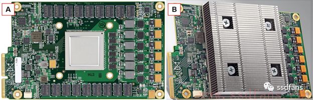
At present, the industrial focus of artificial intelligence has shifted from early deep learning algorithms and frameworks to the AI ​​hardware platform. Google developed a dedicated AI chip - TPU, as shown below.
However, another giant Microsoft has embraced the FPGA as an AI computing platform. At the same time, Amazon and Baidu are also FPGA routes. Baidu integrates CPUs, GPUs, and FPGAs on one board, called "XPU." Amazon's cloud service provides an F1 acceleration platform that provides FPGA acceleration.
Why Microsoft chooses FPGA
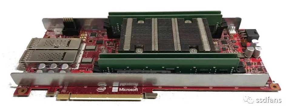
The following figure is Microsoft's FPGA expansion card, called DPU, "Soft DNN Processing Unit".
The Microsoft FPGA strategy is systematic and consists of three main parts:
1. FPGA expansion cards can be interconnected, extended, and integrated into data center services to provide high-bandwidth, low-latency acceleration services;
2. The FPGA is programmable, allowing users to develop their own programs;
3. Microsoft provided a compiler and development environment for its own neural network model, CNTK.
Why did Microsoft choose FPGA? Because Microsoft and Google are two different genes, Google likes to try new technologies, so it is natural to use TPU to pursue the highest performance. However, Microsoft is a company with a very heavy commercial culture. Choosing a solution is a matter of cost-effectiveness and business value. Although a special chip is dazzling, is it really worth it?
The main disadvantage of chip making is the large investment, long time cycle, and the logic inside the chip cannot be modified. Artificial intelligence algorithms have been rapidly iterating, and it takes at least a year or two to do chips, meaning that only old architectures and algorithms can be supported. If the chip wants to support the new algorithm, it must be made general-purpose, provide instruction sets for the user to program, and versatility will reduce performance and increase power consumption, because some functions are wasted. Therefore, although many chip companies have made chips, many products are still made by FPGAs. For example, Bitland's digging machine can no longer support new mining algorithms.
Dumbly spent 8 years ago at Microsoft Asia Research Institute in the accelerated research of Bing search engine with FPGA+Open Channel SSD. At that time, FPGAs could do a few of the streets of CPU learning performance, and at the same time save the cost of purchasing servers and reduce heat dissipation. , land and other costs. So Microsoft chose FPGA based on commercial considerations and long-term accumulation and exploration experience.
Horizontal comparison of CPU, GPU, ASIC and FPGA
Our common hardware computing platforms now include CPUs, GPUs, ASICs, and FPGAs. The CPU is the most versatile, mature instruction set, such as X86, ARM, MIPS, Power, etc. As long as users develop software based on the instruction set, they can use the CPU to complete various tasks. However, CPU's versatility determines that the computing performance is the worst. In modern computers, many calculations require a high degree of parallelism and pipeline architecture. However, despite the long CPU pipeline, the number of computing cores is only a few dozen at most. not enough. For example, watching a high-definition video, so many pixels to be rendered in parallel, the CPU dragged back.
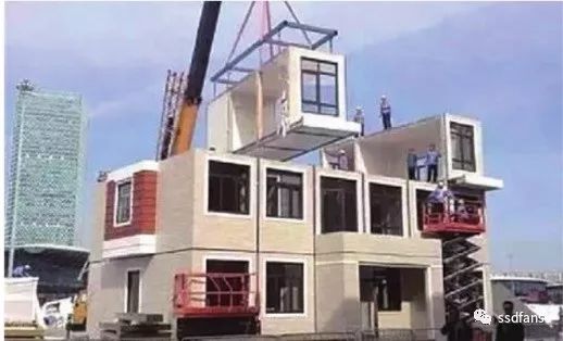
The GPU overcomes the shortcomings of insufficient CPU parallelism and stacks hundreds of thousands of parallel computing cores into a single chip. Users can use GPU programming languages ​​such as CUDA and OpenCL to develop programs using GPUs to speed up applications. However, the GPU also has serious drawbacks, that is, the smallest unit is the computing core, or too large. In computer architecture, a very important concept is granularity. The finer the granularity, the more space users can play. Just like the building, if you use a small brick, you can make a lot of beautiful shapes, but the construction time is long, if you use concrete prefabricated parts, the building will be quickly built, but the style of the building is limited. As shown in the following figure, the prefabricated building is the same as the building block. It will be very fast, but it will be almost the same. It will not work for other buildings that we want to build.
The ASIC overcomes the disadvantage of the coarse GPU granularity, allowing the user to start custom logic from the transistor level and finally to the chip foundry to produce a dedicated chip. No matter if it is performance or power consumption, it is much better than GPU. After all, the design starts from the lowest level, there is no wasted circuit, and the highest performance is pursued. However, ASICs also have a lot of disadvantages: large investment, long development cycle, and the logic of the chip cannot be modified. To make a large-scale chip, you need to invest at least tens of millions to hundreds of millions of dollars. The time cycle is about a year or two. Especially for AI chips, there is no universal IP. Many of them want to develop their own, and the time period is longer. After the chip is ready, if there are big problems or feature upgrades (some minor problems can be solved by the reserved logic to modify the metal layer connection), it cannot be directly modified, and the layout should be re-edited and delivered to the factory.
So, finally, back to the FPGA: taking into account the advantages of ASIC calculation granularity and GPU programmable. The FPGA's computational granularity is fine and can go to the NAND gate level, but the logic can be modified and programmable.
FPGA Getting Started
When we go to college to study computers, we must first learn the basic knowledge of Boolean algebra. Starting from logic gates such as NAND gates, we can build up digital logic such as adders and multipliers. Finally, we combine the first-level stages to achieve very complex computing functions (Dumb Gossip here, Professor Deepin Hinrich is the son of Boer's grandson). In the ASIC, the NAND gates are implemented by transistors, but the transistors cannot be programmed. They must be made into a layout and sent to the chip foundry for use. How can digital logic be programmable? We all know that digital logic can be represented by a truth table. The following figure shows the truth table of a NAND gate.

The FPGA inventor thought of a way to use a lookup table to store the output of a truth table. The following figure is a 3bit XOR gate lookup table, 3bit is a total of 8 states, the lookup table holds the results of each state, the input 3 bits as an index, read directly from the table to the calculation results, through a selection switch Output. This avoids the need to build computational logic and simplifies the chip architecture. It only requires a lot of lookup tables in the chip. Everyone can cascade and combine together to implement complex logic and calculations. The current mainstream FPGA uses SRAM technology, which is to save the status of the lookup table in SRAM.

However, merely having a look-up table is not enough. The root of a digital integrated circuit is a clock, and all the logic is synchronized according to the clock tick. For example, several gangsters have no tactics, but tens of thousands of troops are fighting. If they still fight each other, they will not be able to play the advantages of the group. For example, how do soldiers and soldiers cooperate? How to divide labor between companies? The military operations need to pay attention to the formation method. Ancient Chinese gods of war are familiar with military books, and they will use arrays of the Eight Diagrams and Long Snake Array to command the army to fight in accordance with the unified command. For example, Fazheng collaborated with Huang Zhong, and Ding Junshan set up a good battle against the mountain. Fazheng was standing at the top of the commanding flag. Under his order, the veteran Huang Zhong put the Xiahouyuan into two halves, relying on the formation method. Take the weaker and stronger example. There are hundreds of thousands or even millions of lookup tables in the FPGA, which requires a unified command to act. This is the clock.
The following figure is the basic unit within the FPGA, lookup table + D trigger + selector switch. D flip-flops are used for storage and lookup tables are combinatorial logic. Each clock cycle will output a value, select whether to use a lookup table or a D flip-flop.

If you look at the basic unit of the above FPGA, you understand the basics of the digital circuit - RTL, Register Transfer Level, register transfer level. The digital circuit consists of two basic parts: combinational logic and sequential logic. The combinational logic is the Boolean algebra we discussed earlier. It can be used as a logic operation, but it does not have a memory function. The lookup table in the figure above is the function of combinational logic. Sequential logic is a memory function that can control the input and output according to the clock beat. The D flip-flop in the figure above functions as a memory. We call it a register. In this way, combining combinational logic and sequential logic, we can design a large-scale digital circuit from this level, called RTL design, that is, designing a complex computing system from combinational logic and sequential logic levels.
How can FPGA be programmable?
Then the problem came, how can FPGA be programmable? If you want to control the above basic unit, you need to save several state values ​​of the lookup table, such as a 4-input lookup table, and store 16 bits. At the same time, you need to store a combination logic selection bit and a D flip-flop initial value bit. The FPGA stores these configuration data in the SRAM and configures it in each basic cell. By writing custom data to the SRAM, the entire FPGA logic is programmable.
With the above basic logic unit is not enough, how to cascade a number of basic logic? How is the cascaded connection part programmable?
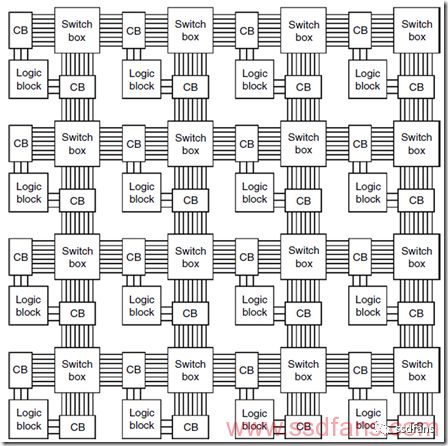
The following figure shows the structure of the interconnection between the logic blocks in the FPGA. The input and output of the logic block is cascaded to other logic blocks through the connection block Connection Block CB and the switching block. The connection block determines the connection line to which the signal of the logic block is connected. The switching block determines which connection line is connected to the logic block. The signal needed by the block is connected to the adjacent logic block. The connection block and the swap block can be programmed based on the SRAM method. Inside the connection block are some selector switches. Inside the swap block are some switches.
It can be seen that the connection line is far more complicated than the logic block. In the modern FPGA chip, the connection generally occupies 90% of the area, and the real logic part has only about 10% area.
FPGA expansion resources
The above combinational logic in the FPGA is not enough, because users sometimes do not want to use their own logic, some commonly used logic directly with the ready-made. So modern FPGAs come with a lot of commonly used computing units, such as adders, multipliers, on-chip RAM, and even embedded CPUs. They are not set up by look-up tables, but are built with transistors like ASICs. This saves chips. Area, and better performance. These calculation units allow users to configure and combine.
For example, a large number of multipliers are used in deep learning. At this time, many multipliers are used inside the FPGA to play a large role. These multipliers and user logic can realize many artificial intelligence calculations and achieve high performance.
China leading manufacturers and suppliers of DC Support Capacitors,DC Capacitor, and we are specialize in Electrolytic capacitor,High Voltage Capacitor, etc.DC Support Capacitors
DC Support Capacitors,DC Capacitor,Electrolytic Capacitor,High Voltage Capacitor
YANGZHOU POSITIONING TECH CO., LTD. , https://www.yzpst.com