Time flies, it has been three years since I first painted the first circuit. Just as you started to touch the board, like you, I was full of doubts and excited. A lot of experience and knowledge about hardware circuits on the Internet is dazzling. Like signal integrity, EMI, PS design will halo you. Don't worry, everything should come slowly. What a hardware engineer needs to do, after reading this article, I believe you will understand.
1) The overall idea. Design hardware circuits, big frameworks and architectures to figure out, but it's not easy to do this. Some big frameworks may have their own bosses and teachers already thinking about it. They just implement the ideas concretely; but some have to design their own frameworks, then you have to figure out what functions to implement, and then find out whether you can achieve the same or similar functions. The reference circuit board (to know how to use the results of others, the more experienced engineers will learn to learn from others' results). 2) Understand the circuit. If you find a reference design, congratulations, you can save a lot of time (including pre-design and post-debugging). Copy now? NO, or understand and understand first, on the one hand can improve our circuit understanding ability, and can avoid errors in the design. 3) Didn't find the reference design? It's ok. First determine the large IC chip, look for the datasheet, see if its key parameters meet your own requirements, which are the key parameters that you need, and whether you can understand these key parameters, are the embodiment of the capabilities of hardware engineers, which also requires long-term The ground slowly accumulates. During this period, you should be good at asking questions. Because you don't understand things, others can wake you up in one sentence, especially hardware design. 4) The hardware circuit design is mainly three parts, schematic, pcb, bill of materials (BOM) table. Schematic design is to convert the previous ideas into circuit schematics. It is very similar to the circuit diagram in our textbook. Pcb involves the actual circuit board, which is based on the schematic diagram converted from the netlist (the netlist is the bridge between the communication schematic and the pcb), and the specific component package is placed (layout) on the circuit board. Then connect its electrical signal (wiring) according to the flying wire (also called pre-wire). After completing the PCB layout and routing, which components should be used, we will use the BOM. 5) What tools are used? Protel, which is altium easy to use, is also popular in China. It is enough for general work, suitable for beginner designers. In fact, whether using simple protel or complex cadence tools, the hardware design is the same (protel operation is similar to windwos, post-command type; and cadence product concept & allegro is pre-command type, used to Protel, suddenly turned to cadence tools, will not be used to this reason). There must be a major part of the design: 1) schematic design. 2) pcb design. 3) Make a BOM. Now briefly talk about the design process (steps):

1) The principle library is established. To put a new component on the schematic, we have to build a library of components. The library defines the pin definitions and their properties of the new component, and is represented in a specific graphical form (we often see a rectangle (representing its IC BODY), surrounded by many short lines (representing IC pins)) . Protel creates libraries and is simple, and because of the large number of people, many components can find ready-made libraries, which is very convenient for users. You should be clear about the differences between ic body, ic pins, input pin, output pin, analog pin, digital pin, power pin. 2) After having a sufficient library, you can draw on the schematic, and connect the relevant components through wire according to the datasheet and system design requirements. Add line and text comments in relevant places. The difference between wire and line is that the former has electrical properties and the latter does not. Wire is suitable for connecting to the same network, and line is suitable for annotation graphics. At this time, you should find out some basic concepts, such as: wire, line, bus, part, footprint, and so on. 3) After this step, we can generate netlist, this netlist is the bridge between the schematic and pcb. The schematic is a form we can recognize. To convert it into a pcb, the computer must convert the schematic into the form netlist it knows, and then process and convert it into pcb. 4) Get the netlist and draw the pcb right away? Don't worry, do ERC first. ERC is an abbreviation for electrical rule checking. It can troubleshoot some basic design errors of the schematic, such as multiple outputs connected together. (But be sure to check your schematics carefully, you can't rely too much on the tools. After all, the tools don't understand your system. It's just purely based on some basic rules.) 5) Get pcb from netlist, a bunch of dense components, And the countless flying lines are not a shock to you? Oh, don't worry, you have to come slowly. 6) Determine the size of the board. Draw a frame in the keepout area (or the mechanism area), which will limit the area of ​​your wiring. It is necessary to consider the length of the board and the width of the board according to the demand (sometimes, it is necessary to consider the thickness of the board). Of course, the laminate has to be considered. (Laminating means that there are several layers in the slab, how to apply it, for example, the board has a total of 4 layers, the top layer takes the signal, the first layer in the middle is laid, the second layer is laid in the middle, and the bottom layer is signaled). Explain the terminology in (2) first. Post-command, for example, we want to copy an object, we must first select the object, then press ctrl + C, then press ctrl + V (copy command occurs after the selected object). This kind of operation windows and protel are used this way. But concept is another way, we call pre-command. Similarly, we have to copy a thing, first press ctrl+C, then select object, and then click outside (the copy command occurs before the selected object). 1) After determining the board frame, the component layout (placement) is very important. It often determines the difficulty of post-wiring. Which components should be placed on the front and which components should be placed on the back should be considered. But these are all problems that benevolent and benevolent, and that wise men see wisdom; they can be placed differently from different angles. In fact, I have drawn the schematic diagram, understand all the components, and naturally have a clear understanding of the component placement (if you let a person who is not drawing a schematic to place the component, the result will often surprise you ^_^). For the first entry, pay attention to the analog components, the isolation of the digital components, and the placement of the mechanical position, while paying attention to the topology of the power supply. 2) The next step is wiring. This is often interactive with the layout. Experienced people often see where they can be successfully routed at the beginning. If it is difficult to route in some places, you need to change the layout. For fpga designs, the schematics are often modified to make the wiring smoother. There are many factors involved in wiring and layout problems. For high-speed digital parts, they are complicated by the problem of signal integrity, but often these problems are difficult to quantify or even difficult to calculate. Therefore, in the case that the signal frequency is not very high, the first principle should be the same. 3) OK? Don't worry, check with DRC first. This is a must check. The DRC will mark the coverage of the wiring and the violation of the rules, and correct it according to this one-by-one troubleshooting. 4) Some pcbs also need to be coated with copper (which may lead to increased costs), and the outlet part will be made into teardrops (the factory may help you). The final pcb file is converted to a gerber file and can be delivered to pcb production. (Some directly to pcb, the factory will help you turn gerber). 5) To assemble the pcb, prepare the bom table, which can be directly exported from the schematic. However, it should be noted that in the schematic diagram, which parts of the components should be on and which components should not be on, it is necessary to have a psychological number. For small batches or research boards, it is also convenient to use excel to manage it yourself (large companies often have professional software to manage). For the novice, the first version is not recommended to be directly handed over to the assembly plant or the welding factory to weld all the bom materials, which is not convenient for troubleshooting. The best way is to prepare the components yourself according to the bom table. After the board comes, step by step on the components and debug. . . Talk about debugging 1) Get the first step of the board, do not rush to see the power supply function, hardware debugging can not be completed in one step. First take a multimeter to see if the key network is not normal, mainly to see if there is a short circuit between the power supply and the ground (although the manufacturer has already done the test for you, this step still has to look at it yourself, sometimes it seems that some steps It is very cumbersome, but it can save you a lot of time!), in fact, the short circuit is not only related to pcb, it may cause this problem in any part of production and production, IO short circuit generally does not cause catastrophic consequences, but the power supply is short-circuited. . . . . . 2) The power supply network is not short-circuited? So good, then look at whether the power output is its ideal value. For beginners, it is best to use one chip on the IC when debugging. The first one is the power chip. 3) Is the power supply network shorted? This is more troublesome, but it is necessary to take a closer look at whether the schematic diagram of the schematic is possible. At the same time, combined with the method of secant, step by step to check where the bottom is short-circuited, it is a problem of pcb (the general bad pcb factory may appear This situation), or the problem of assembly, or the problem of own design. There are some tips on checking for shorts, which will be logged out in the future. . . . . . 3) The power chip has no output? Check to see if your power chip input is normal. Also check the place where there is an enable signal, a voltage divider resistor, and a feedback network. . . . . . 4) Is the output value of the power chip not in the expected range? If it is very outrageous, such as 10%, then look at the voltage divider resistors, these two voltage divider resistors generally use 1% accuracy, this you did not, and look at the feedback network, it will also affect you The range of output power. 5) The power output is normal, don't be happy, if there are conditions, take the oscilloscope and see if the output jump of the power supply is normal. That is to grasp the moment of power-on, look at the situation of the power supply from scratch (as to why you have to look at it, oh... Professionals still have to see ~) talk about the power supply is undoubtedly the power supply design is the entire circuit The most important part of the board. The power supply is unstable, don't talk about other tricks. I don't think balabala tells how important it is. The most common use in power supply design is to obtain a stable "low" voltage from a stable "high" voltage. This is also known as DC-DC (DC-DC), and there are two types of power regulator chips that are used most in DC-DC. One is called LDO (Low-Dropout Linear Regulator, which we will say later) The voltage source is also referred to as it), and the other is called PWM (Pulse Width Modulation Switching Power Supply, which we also refer to in this article as switching power supply). We often hear the efficiency of PWM is high, but the response of LDO is fast, why is this? Don't worry, let's take a look at their principles. The following will involve some theoretical knowledge, but it is still very easy to understand, if you don't understand, hey, you have to check your own foundation.

First, the working principle of the linear regulated power supply is a simple schematic diagram of the internal structure of the linear regulated power supply. Our goal is to get a low voltage Vo from the high voltage Vs. In the figure, Vo is divided by two voltage divider resistors to get V+, V+ is sent to the positive terminal of the amplifier (we call this amplifier the error amplifier), and the negative terminal Vref of the amplifier is the reference level inside the power supply (this reference The level is constant). The output Va of the amplifier is connected to the gate of the MOSFET to control the impedance of the MOSFET. When Va becomes larger, the impedance of the MOSFET becomes larger; when Va becomes smaller, the impedance of the MOSFET becomes smaller. The voltage drop across the MOSFET will be Vs-Vo.
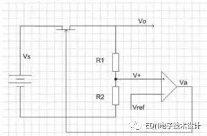
Now let's see how stable Vo is. If Vo becomes smaller, then V+ will become smaller, and the output Va of the amplifier will also become smaller. This will cause the impedance of the MOSFET to become smaller, so that after the same current, the voltage difference of the MOSFET will be It becomes smaller, so Vo is lifted up to suppress the decrease of Vo. Similarly, Vo becomes larger, V+ becomes larger, Va becomes larger, and the impedance of the MOSFET becomes larger. After the same current, the voltage difference of the MOSFET becomes large, thereby suppressing Vo from becoming large. Second, the working principle of the switching power supply
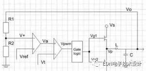
As shown above, in order to obtain Vo from the high voltage Vs, the switching power supply adopts a square wave Vg1 with a certain duty ratio, Vg2 pushes the upper and lower MOS transistors, Vg1 and Vg2 are inverted, Vg1 is high, Vg2 is low; upper MOS tube When turned on, the lower MOS transistor is turned off; when the lower MOS transistor is turned on, the upper MOS transistor is turned off. Therefore, a square wave voltage with a certain duty ratio is formed at the left end of L. The inductance L and the capacitance C can be regarded as a low-pass filter, so that the square wave voltage is filtered to obtain the filtered stable voltage Vo. After V is divided by R1 and R2, it is sent to the negative terminal V+ of the first amplifier (error amplifier), and the output Va of the error amplifier is used as the positive terminal of the second amplifier (PWM amplifier). The output of the PWM amplifier Vpwm is one. A square wave with a certain duty cycle is processed by the gate logic circuit to obtain two inverted square waves Vg1 and Vg2 to control the switching of the MOSFET. Third, the linear regulated power supply and the switching power supply have a better understanding of the working principle of the linear regulated power supply and the switching power supply, we can understand why the linear regulated power supply has less noise, faster transient response, but the efficiency is poor. The switching power supply is noisy and the transient response is slow, but the efficiency is high. The linear regulated power supply has a simple internal structure and a short feedback loop, so the noise is small and the transient response is fast (when the output voltage changes, the compensation is fast). But because the input and output voltage differences all fall on the MOSFET, it is inefficient. Therefore, linear regulation is generally used in applications where low current is required and voltage accuracy is high. The switching power supply has a complicated internal structure, many factors affecting the performance of the output voltage noise, and its feedback loop is long, so its noise performance is lower than that of the linear regulated power supply, and the transient response is slow. However, according to the structure of the switching power supply, the MOSFET is in both fully open and fully closed states. Except for driving the MOSFET and the energy consumed by the MOSFET's own internal resistance, all other energy is used for the output (in theory, L and C are not consumed). Energy, although this is not the case, these energy consumption is small). First write part 8, wait until the picture can be uploaded and then add part 6,7 as a description of the switching power supply principle, and LDO compared with the switching power supply. This part clarifies some of the misunderstandings of high-speed signal recognition. First, the high-speed look at the signal edge, not the clock frequency. 1) Generally speaking, when the clock frequency is high, the rising edge of the signal is fast, so generally we regard them as high-speed signals; but the reverse is not necessarily true, the clock frequency is low, if the rising edge of the signal is still fast, the same should be taken Treated as a high speed signal. According to the signal theory, the rising edge of the signal contains high-frequency information (using Fourier transform, we can find the quantitative expression), so once the rising edge of the signal is steep, we should deal with the high-speed signal, the design is not good, it is likely to rise. The edge is too slow, there is overshoot, undershoot, and ringing. For example, the I2C signal, in ultra-fast mode, has a clock frequency of 1MHz, but its specification requires that the rise or fall time does not exceed 120ns! There are indeed a lot of boards I2C can't pass! 2) Therefore, we should pay more attention to the signal bandwidth. According to the empirical formula, the relationship between bandwidth and rise time (10%~90%) is Fw * Tr = 3.5 2. Oscilloscope selection 1) Many people have noticed the sampling rate of the oscilloscope and did not notice the bandwidth of the oscilloscope. But often oscilloscope bandwidth is a more important parameter. Some people think that as long as the oscilloscope sampling rate meets more than twice the signal clock frequency, this is a big mistake. The cause of the error is the wrong understanding of the sampling theorem. Sampling Theorem 1 shows that when the sampling frequency is greater than twice the maximum bandwidth of the signal, the original signal is perfectly restored. However, the sampling theorem refers to a signal with a band-limited signal (the bandwidth is limited), which is seriously inconsistent with the actual signal. Our general digital signal, except for the clock, is not periodic. From a long time, its spectrum is infinitely wide; to capture high-speed signals, it cannot be too much distortion of its high-frequency components. The oscilloscope bandwidth metrics are closely related to this. Therefore, the real thing to note is that the rising edge distortion of the signal captured by the oscilloscope is within our acceptable range. 2) So what is the right choice for a high-bandwidth oscilloscope? In theory, an oscilloscope with 5 times the signal bandwidth captures less than 3% of the original signal. If you want to lose more lenient, you can choose a lower-end oscilloscope. An oscilloscope that uses three times the signal bandwidth should meet most of the requirements. But don't forget the bandwidth of your probe!
10 Mm Nano Tip,Smart Board Touch Screen Pen,Electronic White Board Pen,Infrared Touch Screen Pen
Shenzhen Ruidian Technology CO., Ltd , https://www.szwisonen.com