In 2004, the European Telecommunications Standards Institute (ETSI) proposed the new digital trunking communication system DMR (Digital Mobile Radio). Compared with the TETRA and iDEN systems, the DMR system has the advantages of easy implementation and low cost, and has begun to receive large-scale cluster equipment at home and abroad. Manufacturers attach great importance to it. Therefore, this paper proposes a receiver design specifically for the DMR system. It uses two down-conversions for the RF signal, and successively obtains two intermediate frequency signals of 45.05 MHz and 455 kHz, and finally demodulates by the frequency-determining chip TA31 136. voice signal. The solution has the advantages of low cost, good performance, high receiving resolution and wide coverage, and has been successfully applied to the DMR digital terminal equipment we developed.
This article refers to the address: http://
1 Overall design of the receiver Two of the BPFs are discrete components and ceramic filters. The MCF is constructed using finished components and IF AMP is a triode, which will not be described in detail here. The following is a detailed description of the design of each important module.

(1) Circuit design of low noise amplifier LNA.
This receiver is used in actual batch products, which is in consideration of cost reduction. The low noise amplifier LNA is realized by MOS tube 3SK318 and peripheral circuits, and its circuit diagram is shown in Fig. 2.
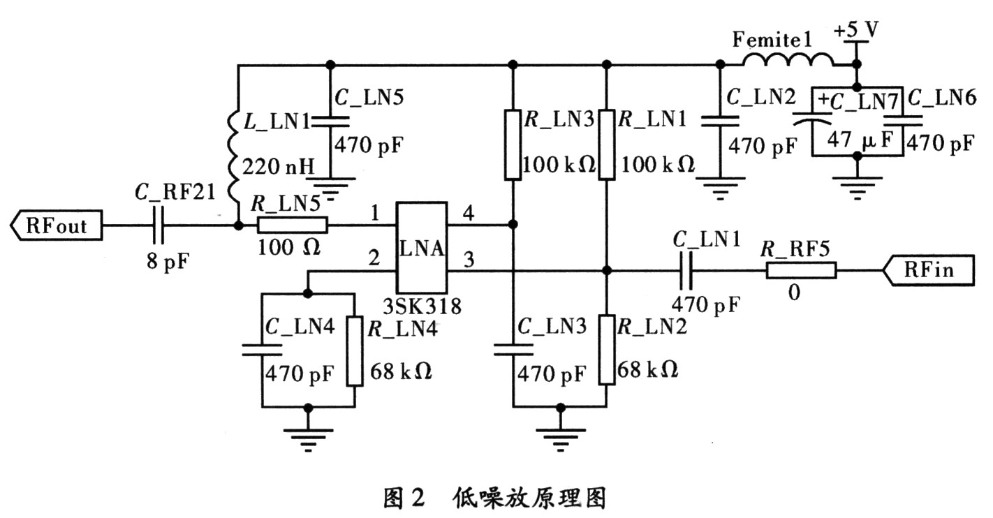
By adjusting the 3SK318's paranoid circuit, when the supply voltage is 5 V, there are V1=4.91 V, V2=4.81 V, V3=0.99 V, V4=2.0 V, at this time, LNA The amplification gain is 20 dB.
(2) Receiver local oscillator phase-locked loop circuit design.
The local oscillator of this receiver is provided by a phase-locked loop frequency synthesizer consisting of the MAX2620 and MB15E03L. Maxim's MAX2620 is a very convenient oscillator chip with its internal components, as shown in Figure 3(a). The MAX2620 provides a buffered-amplified output stage that reduces the effects of load variations on the oscillator frequency. The supply voltage ranges from 2.7 to 5.25 V. A bias circuit is provided internally to stabilize its operating point, causing operation to fluctuate. The effect is reduced and has a power-off capability, controlled by the SHDN terminal. The two complementary outputs (OUT and OUT) can form two single-ended outputs or one differential output. The MAX2620 uses bipolar technology and the output is open-collector, so the output requires a pull-up resistor. The two-phase output power is up to -2 dBm and -10 dBm for different loads. In this design, OUT outputs the FM signal, and the OUT output is used as the PLL feedback frequency for phase discrimination.
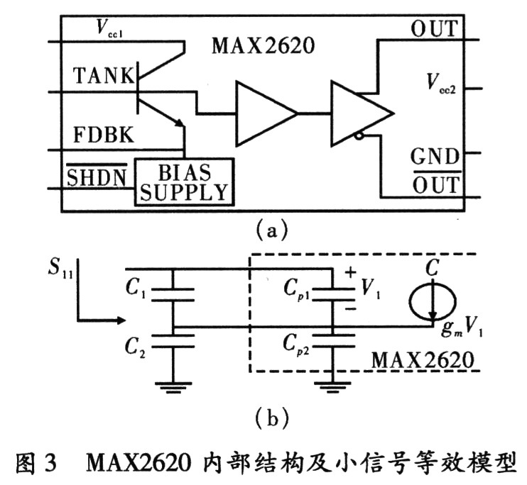
The voltage-controlled oscillator is designed using the traditional Colpitts common-emitter series resonant structure, which operates over a wide frequency range to meet system bandwidth requirements. The MAX2620 uses a bipolar design with an AC small-signal equivalent circuit, as shown in Figure 3(b). Capacitors C1, C2, parasitic capacitances Cp1, Cp2, and transconductance gm determine the input impedance of the oscillator. 
The Colpitts oscillator uses the "negative resistance" principle to achieve oscillation. After obtaining the input impedance of the active circuit and the single port network parameter S11, an LC resonant tank corresponding to the active portion is constructed. The overall structure of the VCO is shown in the MAX2620 section of Figure 4. After the VCO is built, the VCO oscillation frequency range is measured from 420 to 470.
The Colpitts oscillator uses the "negative resistance" principle to achieve oscillation. After obtaining the input impedance of the active circuit and the single port network parameter S11, an LC resonant tank corresponding to the active portion is constructed. The overall structure of the VCO is shown in the MAX2620 section of Figure 4. After the VCO is built, the measured VCO oscillation frequency range is 420 ~ 470 MHz @ 0 ~ 4 V, the modulation sensitivity is 12.5 MHz / V, and the linearity is good. The MAX2620 integrates a VCO buffered amplifier output stage to reduce the effects of load changes on the oscillator's oscillation frequency. The output is matched to the 50Ω load by boosting the inductor and series capacitors. The OUT terminal requires only a 50Ω boost resistor and is coupled back to the frequency synthesizer.
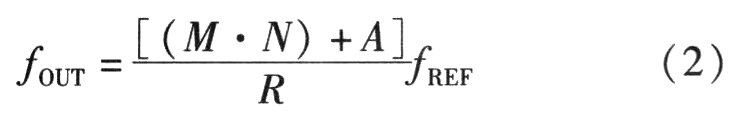
After the VCO is completed, the chip design loop filter is synthesized according to the PLL frequency of the selected path. The PLL frequency synthesis chip MB15E03SL is a serial input swallow pulse PLL frequency synthesizer manufactured by Fujitsu. It supports a working frequency of up to 1.2 GHz. It integrates a low noise digital phase detector and can set the dual mode scale factor M/M+. 1,14 bit programmable reference divider ratio R and 18 bit programmable N divider, the chip provides a very simple three-wire SPI serial input to set the above parameters to get the desired frequency, the output frequency is calculated as
For other parameters of MB15E03SL, please refer to the data sheet and the schematic diagram of the phase-locked loop frequency synthesizer, as shown in Figure 4.
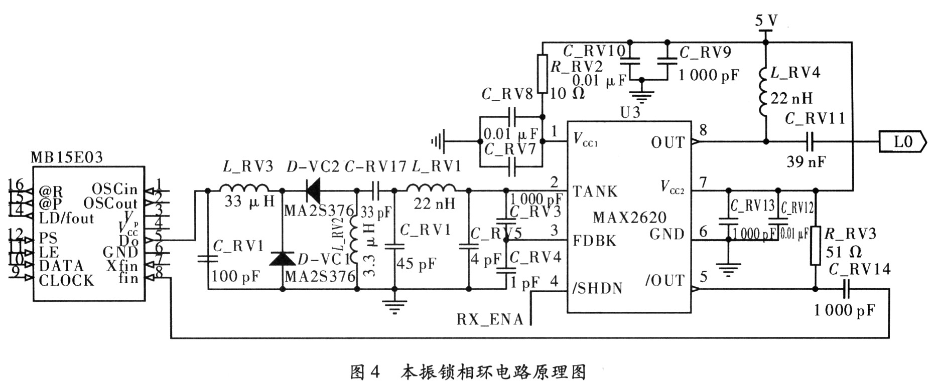
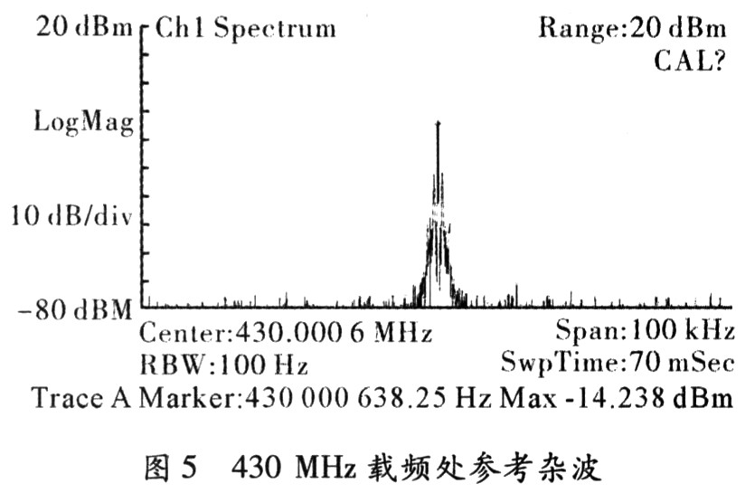
According to the system requirements: channel spacing 12.5 kHz, tolerance ± 2 ppm, lock time < 4 ms, according to the literature [2] calculated loop bandwidth must meet Fc ≥ 1.6 kHz. Since the increase of the loop bandwidth can reduce the lock time, and the loop is too wide, the phase noise is seriously affected, and it is generally required that the Fc does not exceed 1/5 of the comparison frequency FPD, and Fc=2.5 is selected. kHz. The sensitivity of the VCO modulation is equal to 20 MHz/V, the charge pump gain is selected as Kφ=±1.5 mA, the comparison frequency fPD=1 2.5 kHz, the output frequency range is 420-470 MHz, and the loop filter bandwidth Fc=2. 5 kHz, phase margin φ=48°, loop filter pole ratio T3/T1=45%, and the parameters of the loop filter are calculated with reference to the input frequency of 13 MHz. The loop filter parameters are obtained as follows: R_LF1=3.3 kΩ, R_LF2=5.6 kΩ, C_LF1=4.7 nF, C_LF2=47 nF, C_LF3=2.2 nF. The theoretical calculation results show that the phase-locked loop lock time Lock-time=1.3 ms under this loop condition, the phase noise can reach PN=-94.07 dBe/Hz@10 kHz, and the loop bandwidth Fc=2.56 kHz, the phase margin is 39.52°, which has been able to meet the system requirements. The schematic diagram of the FM phase-locked loop is established according to the loop filtering condition, as shown in Fig. 4. Figure 5 shows the clutter test diagram for a phase-locked loop of 430 MHz.
(3) Downconverting mixer circuit design.
Maxim's MAX2680 is a low power, low noise figure, specifically designed for low voltage operation downconverting mixers. It is suitable for frequencies from 400 to 2 500 GHz, with a supply voltage of 2.7 to 5.5 V, a high third-order input cut-off point (IIP3 at 2 450 MHz) and a low power shutdown mode of <0.1 μA. It is an ideal device for handheld communication devices, so this design uses this chip. Circuit design, as shown in Figure 5.
The receiver uses two down-conversions for frequency discrimination. The MAX2680 is the first down-conversion to generate a 45.05 MHz IF signal. /SHDN is the switch control enable terminal. When it is low level, the chip does not work. When it is high level, the chip works normally. The received RF signal range is 400-450MHz, which satisfies the applicable range of the MAX2680. The local oscillator signal L0 is generated by a phase-locked loop mixer. Theoretically, when the RF is 400 MHz and the L0 is 445 MHz, the gain of the mixing is 11 dB; and the actual measurement: when the RF is 405 MHz, the power is -48 dBm, the L0 is 450.05 MHz, and the power is -16. At dBm, the output IF is 45.05 MHz and the power is -54 dBm. The power signal requirements of the subsequent modules (required for the input signal by the frequency discrimination chip TA31136) are met.
(4) Circuit design of the discriminator.
The TA31136 is a low voltage operated FM IF detection chip that is primarily suitable for use in wireless telephones. The TA31136 operates from 1.8 to 5.5 V and contains a 2ndIF mixer with an input IF signal of 10 to 100 MHz, a noise detection circuit, a high gain limiting IF amplifier and a ceramic. The integral discriminator can be applied to the middle of the week, and the chip also has the RSSI function. Since the receiver uses two down-conversion frequency discrimination, the second down-conversion and frequency discrimination can be implemented in the TA31136. Therefore, the design uses the frequency-determining chip and the discriminator circuit design, as shown in FIG.
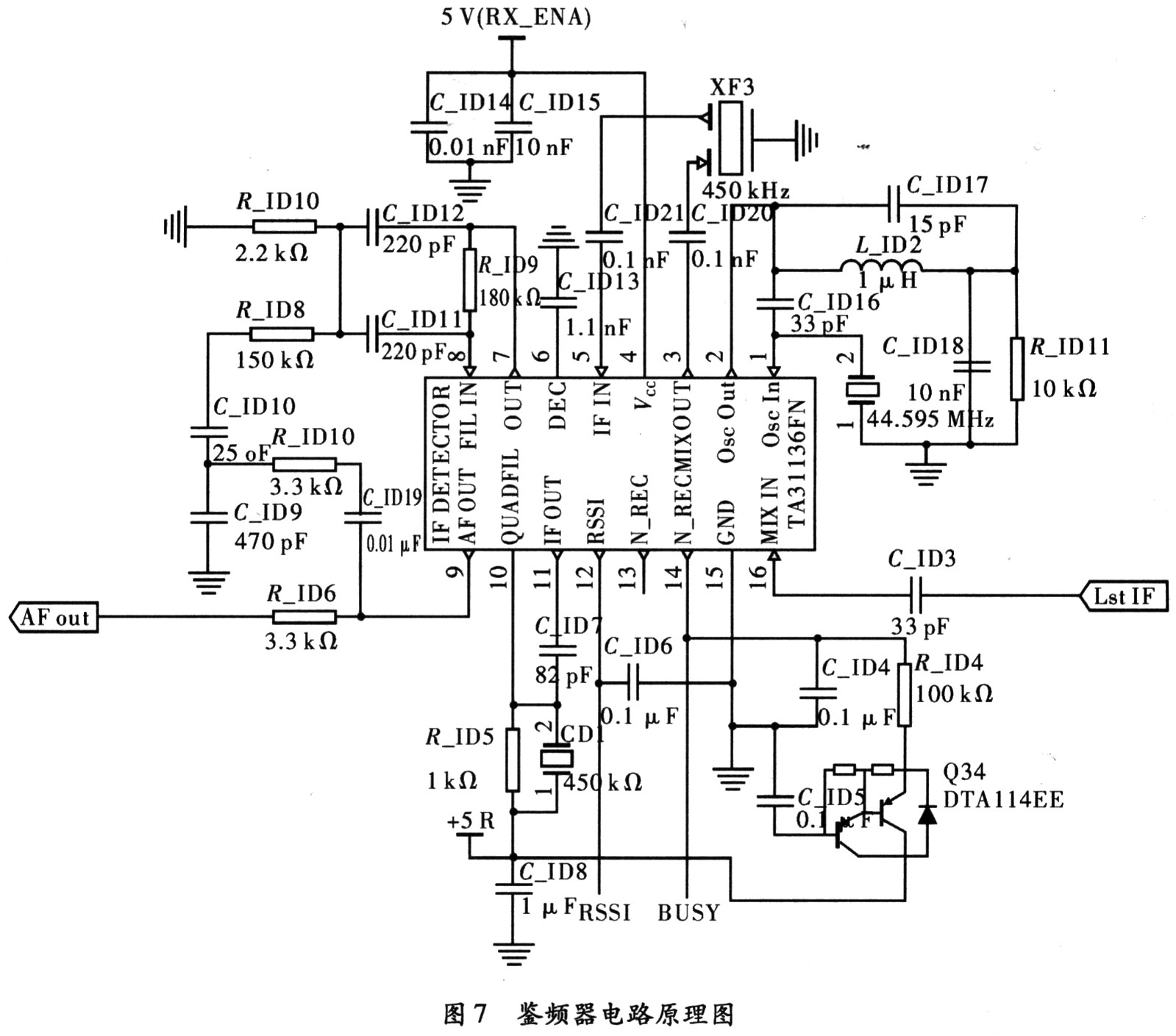
The first down-conversion of the 45.05 MHz IF signal generated by the MAX2680 is filtered through the crystal filter to filter the adjacent clutter signal, amplified by the IF amplifier, and entered from Pin16 of the TA31136, and the 44.595 MHz signal generated by the crystal oscillator. Mixing produces a second intermediate frequency signal of 455 kHz. The 455 kHz IF signal is filtered from the Pin3 output via the ceramic filter XF3, then from the Pin5 to the IC, amplified by the IF amplifier inside the IC, input to the integrated discriminator for demodulation, and finally output a speech signal through an LPF. Part of the audio signal output by TA31136 enters the Pin7 and Pin8 of the IC through a voltage dividing circuit, and the noise component is amplified and rectified by a filter and amplifier inside the IC to generate a DC voltage signal corresponding to the noise component, and the DC voltage signal and From the MCU internally set voltage value comparison size, the MCU outputs high and low voltage signals according to the comparison result to control Pin14 of TA31136 to realize the opening and closing of the squelch when receiving the signal.

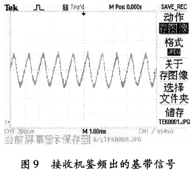
Figure 9 shows the baseband signal sampled by the receiver. It can be seen that the demodulated signal has little distortion. The receiver passes the test, and the error between the signal and the original signal is <1%, which is in compliance with the wireless communication requirements. The power of the input FM signal is changed. When the frequency is -80 dBm, the frequency-resolved signal can be output. When it is <-80 dBm, the frequency cannot be discriminated, which is the receiver's receiving sensitivity.
3 Conclusion The actual DMR receiver was fabricated on a 20-cm × 10 cm 4-layer printed board with copper on the surface and a supply voltage of 5 V. The FM receiver constructed by 3SK318, MAX2680, MAX2620, MB15E03SL and TA31136 has the characteristics of small influence from external distribution parameters, convenient debugging and low cost. It has been successfully applied in the prototype of DMR digital terminal equipment developed.
Digital display meter is the abbreviation of digital display instrument. LED and LCD are commonly used as display elements.
Digital display meter has the characteristics of visual intuition, convenient setting and high degree of intelligent control. In addition, with the rapid development of current sensing technology, the function of digital display instrument is becoming more and more powerful and the accuracy is constantly improving. Digital display instrument is replacing traditional mechanical instrument in a large number and has been widely used in all walks of life and daily life.
Digital Display Meter,Digital Display Intelligent Meter,Electrical Connection Digital Display Meter,Intelligent Digital Panel Instrument
Taizhou Jiabo Instrument Technology Co., Ltd. , https://www.taizhoujiabo.com