As technology advances, EMI poses an increasing threat to the proper functioning of circuits. This is because electronic applications are turning to various wireless communications or portable platforms. Therefore, most interfering EMI signals eventually enter the PCB trace in the form of conducted EMI.
When you're trying to design an EMI-resistant circuit, you'll find that analog Sensor circuits tend to be huge EMI absorbers. This is because sensor circuits often generate low-level signals and have many high-impedance analog ports. In addition, these circuits use a more compact component spacing that makes the system easier to intercept and conduct noise interference into the traces.
In this EMI case, an operational amplifier (op amp) becomes a primary target. We saw this effect in Part 1 of this series, "How EMI Passes Through Media Interference Circuits." (For details of the article, please visit TI's official website: http://www.TI.com.cn/general/cn/docs/gencontent.tsp?contenTId=152156). The EMI signal shown in Figure 1 causes an offset voltage of 1.5 volts. error!
A standard op amp has 3 low impedance pins (positive power, negative power and output) and 2 high impedance input pins (see Figure 1a). Although these pins are resistant to EMI, the input pins are the most vulnerable.
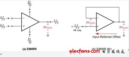
Figure 1 Comparison of EMIRR and EMIRR IN+ determination methods
EMIRR electromagnetic interference suppression ratio
The characteristics of the inverting and non-inverting pins of the voltage feedback amplifier are basically the same. However, the amplifier EMI tolerance test for the non-inverting input (see Figure 1b) is the simplest.
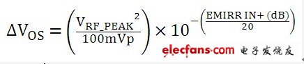
Equation 1
In Equation 1, VRF_PEAK is the peak value of the RF voltage used, VOS is the DC offset voltage of the amplifier, and 100 mVP is the 100 mVP input signal EMIRR IN+ reference.
You can compare the EMI suppression performance of your amplifier with the EMIRR metric. Figure 2 shows the EMIRR IN+ response of the TI OPA333 CMOS op amp. This figure shows that this device can better suppress the frequency signal above the 300 kHz bandwidth of the device.
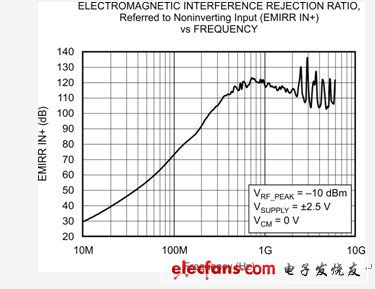
Figure 2 OPA333, EMRR IN+ and frequency
The integrated circuit internal EMI filter has three advantages over the external RC filter. Potential users can test the performance of amplifiers with integrated filters to ensure EMI suppression over a wide frequency range (2). Passive filter components are not ideal for parasitic capacitance and inductance, which limits the ability of the filter to reject very high frequency noise. In contrast, the electrical characteristics of integrated circuits and on-chip passive components are well matched. Finally, integrated circuits using internal filters can also provide customers with other benefits such as fewer components, lower cost, and smaller board area.
To reduce the EMI sensitivity of the circuit, board designers should always pay attention to using a good layout method. This can be achieved by making the trace length as short as possible, using surface mount components, and using a printed circuit board (PCB) with a dedicated signal loop ground plane. Keep the ground plane intact and keep the digital signal away from the analog signal path. In addition, place the RF bypass capacitor on all integrated circuit power pins. Keep these capacitors close to the device pins and ensure that their impedance is as close as possible to 0 ohms at potential EMI frequencies.
CCTV Microphone,Microphone For Security Camera,Cctv Audio Microphone,CCTV Audio Picker
Chinasky Electronics Co., Ltd. , https://www.chinacctvproducts.com