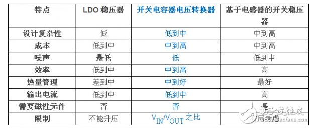
Charge pumps (or switched capacitor voltage converters) fill the gap between linear regulators and inductor-based switching regulators, providing an alternative design option for engineers who don't like inductors. Compared to LDOs, charge pumps require an extra capacitor ("floating" capacitor) to operate, but generally only a slight increase in cost, while the charge pump has a higher output noise level and the output current capability is usually weaker. . However, charge pumps also have advantages that are not available in linear regulators, such as higher efficiency, better thermal management due to higher efficiency operation, the ability to boost and step down, or generate negative voltages. When compared to conventional switching regulators, the charge pump's output current capability is weak and inefficient. But the charge pump is simpler, easier to design, and does not require an inductor. Recent advances in process technology have enabled the input voltage range of charge pumps to be expanded relative to previous generations. Table 1 compares the key performance parameters for each of the above topologies.
Table 1: Performance Comparison of LDOs, Charge Pumps, and Switching Regulators
The charge pump IC uses a capacitor as an energy storage element to generate an output voltage. For example, consider the basic "voltage doubler" charge pump circuit shown in Figure 1. The circuit uses a single floating capacitor (CFLY in the figure) and four internal switches driven by a two-phase clock (with a circle of “xâ€) to produce an output voltage that is twice the input voltage. In the first phase of the clock (θ1 in the figure), a pair of switches charge the floating capacitor to the input voltage (VIN). In the second phase of the clock (θ2 in the figure), the third switch connects the negative terminal of the capacitor to VIN, effectively generating 2 * VIN at the positive terminal of the capacitor. The fourth switch connects the positive terminal of the floating capacitor to the output capacitor. Under no-load conditions, charge is transferred to the output capacitor in each cycle until the output is charged to 2 * VIN, resulting in an input voltage equal to twice the input voltage. When there is an output load, the output capacitor (COUT in the figure) provides the load current on the first phase, while on the second phase, the floating capacitor provides the load current and charges the output capacitor. In order to transfer the charge, the output will settle at a voltage slightly below 2 * VIN. The output capacitor's charge and discharge on two clock phases produces an output ripple that is a function of the output capacitor value, clock frequency, and output load current.
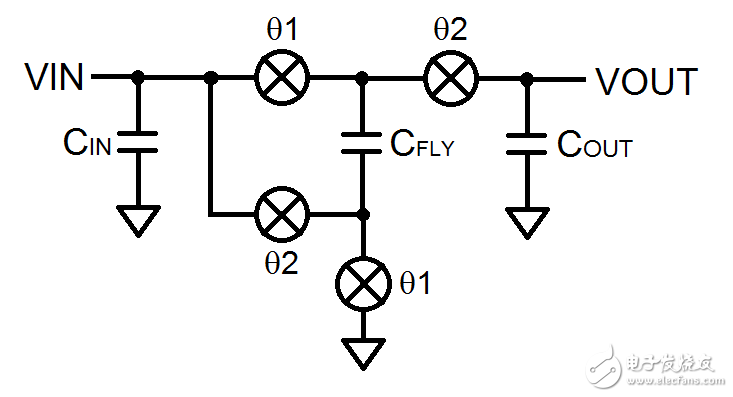
Figure 1: Basic charge pump voltage doubler circuit
All other charge pump circuit topologies are based on this basic circuit, just adding/changing switches and capacitors and the number of clock phases. Depending on the controller and circuit topology, the charge pump can produce an output voltage of any size, such as 2x, 3x the output voltage of the input voltage, an output voltage equal to half the input voltage, a negative output voltage, and the input voltage component. A proportional output voltage, such as an output voltage equal to the input voltage of 3/2, 4/3, 2/3. The efficiency of the charge pump can be very high when approaching the ideal charge ratio. In the above example of a voltage doubler, ideally, the input supply current is equal to twice the output load current and the input power is equal to the output power. The reality is that the efficiency is slightly lower than ideal due to static operating current and other losses. Charge pumps are versatile and can be used in a variety of applications and market segments. The charge pump is more rugged thanks to an innovative design approach that creates opportunities for harsh industrial and automotive environments.
Automotive and industrial design challengesDesigning electronic systems for automotive applications is challenging for a wide range of reasons, including a wide operating temperature range, stringent EMI (electromagnetic interference) and transient requirements, and the high quality required by automotive OEMs (original equipment manufacturers). The car dashboard is very crowded and stuffed with electronics. To make matters worse, there are various wireless systems ranging from Bluetooth to mobile-based network connections. Therefore, it is imperative to add any component to this heat-limited environment, taking care not to generate excessive heat or too much EMI. There are stringent electromagnetic compatibility (EMC) requirements for radiated and conducted electromagnetic interference, radiation and conductivity or radiation and conduction sensitivities, and electrostatic discharge (ESD). The ability to meet these requirements affects the multiple capabilities of IC design. The low EMI and low noise output of the charge pump (no magnetic components, no inductors) make it ideal. Charge pumps are generally less EMI than inductive switches because the floating capacitor connections can be minimized to reduce capacitive coupling and antenna effects. Inductors tend to be larger than capacitors and act like antennas, especially when unshielded. In reality, the floating capacitor output does not produce higher EMI at all compared to a typical digital output. In fact, they produce lower EMI because board traces are minimized.
Creative Led Display,Creative Led Screen,Creative Stage Led Display,Platform Creative Led Display
ShenZhen Megagem Tech Co.,Ltd , https://www.megleddisplay.com