(a) emitter bias difference (b) current source bias difference
The differential has two input terminals and two output terminals, so the input and output of the signal are both double-ended and single-ended. For double-ended input, the signal is applied to both inputs simultaneously; for single-ended input, the signal is applied between one input and ground, and the other input is grounded. For double-ended output, the signal is taken between the two outputs; when single-ended, the signal is taken from one output to ground. Therefore, the differential amplifier circuit has four applications of double-ended input double-ended output, single-ended input double-ended output, double-ended input single-ended output, and single-ended input single-ended output. The above two circuits are double-ended input double-ended output mode.
Input resistance analysis of differential amplifier circuit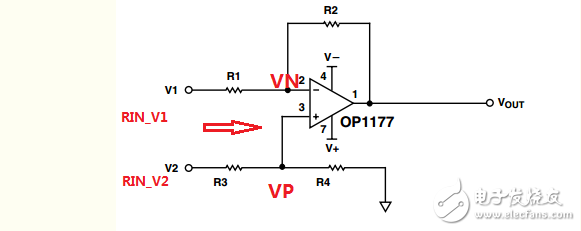
Figure 1 Classic differential circuit input resistance analysis
Also assume that the following conditions are true:
(1) Op amp ideal
(2) Resistance matching, set R1=R2=R3=R4=10KΩ
Let RIN_V2 and RIN_V1 be the input resistances seen in the circuit from the V2 terminal and the V1 terminal, respectively.
As shown in Figure 1, the input resistance of the V2 terminal is relatively simple, and it can be directly seen that RIN_V2=R3+R4. Since no current flows in the 3 terminals of the op amp, it can be obtained:
RIN_V2=R3+R4
=20KΩ
The following focuses on how RIN_V1 is obtained:
Assuming that the signal source V1 is added to the V1 terminal and the current I is generated at the input of V1, in theory, RIN_V1 can be expressed as:
RIN_V1=U/I
From Figure 3 you can get:
I=(U-VN)/R1
And VN=VP=V2*R4/(R3+R4)
From equations (16) to (18), we can get:
RIN_V1=V1*(R3+R4)*R1/(V1*R3+V1*R4-V2*R4)
Substituting into (8)~(9) and finishing, get:
RIN_V1=(2*K2-K1(R3+R4)*R1)/((2*K2-K1)(R3+R4)-(2*K2+K1)R4)----(20)
K1=V2-V1-------------------VCOM differential signal between two sets of input signals
K2=(V2+V1)/2--------------VDEF represents the common mode signal between the two sets of signals
It can be seen from equation (20) that the magnitude of the influence of RIN_V1 is related to the resistance value, the differential mode signal VDEF, and the magnitude of the common mode signal VCOM.
Consider a simple case where the common mode signal VOCM is zero, ie K2=0.
Bring into (20), you can get:
RIN_V1=K1*(R3+R4)*R1/(K1(R3+R4)+K1R4)
=(R3+R4)*R1/(R3+2*R4)
=6.666KΩ
to sum up:
(1) The performance of the differential circuit composed of the op amp and the separation resistor is related to the operational amplifier, the resistance matching degree, etc., and various factors need to be considered in the actual design.
(2) The input resistance values ​​of the two input terminals of the differential amplifying circuit are inconsistent, which affects the performance of the differential amplifying circuit.
It is precisely because of the shortcomings of the classic differential amplifier circuit that better differential amplifiers, instrumentation amplifiers, etc. appear.
xcool vape enjoy free, Disposable Vape Pen brand
Xcool vapor disposable vape pen, xcool vapor hnb, xcool vapor cbd
Shenzhen Xcool Vapor Technology Co.,Ltd , http://www.xcoolvapor.com