The frequency multiplier is an electronic component that can complete the frequency multiplication function of the input signal. In an electronic device with a high operating frequency and strict frequency stability, it is difficult to meet the requirements with a general LC oscillator. If a highly stable crystal oscillator is used, The frequency stabilization requirement can be easily realized by multiplying the frequency.
In the frequency synthesizer, using the harmonic frequencies generated in the frequency multiplier, the stable frequency output with small step interval and many points can be obtained by frequency synthesis, which can be conveniently used in the fields of radar, communication, measurement, etc. . The frequency multiplier can also be used to make a millimeter wave signal source, which has a wide range of applications in millimeter wave communication, military investigation, and guidance.
2 frequency multiplier principleIn theory, any nonlinear original can be used to achieve frequency multiplication. From the working principle, it can be divided into nonlinear reactance (capacitance) type and nonlinear conductance (capacitance) type. When a sinusoidal wave is used to drive a nonlinear component, the output of the nonlinear component is generated at the output end, and the desired harmonic component can be selected by an appropriate filter to achieve the frequency multiplication of the input signal. Commonly used nonlinear frequency doubling components are diodes, transistors, and the like.
The implementation of the frequency multiplier is various. Generally, the following six methods are used to achieve the frequency multiplication: (1) the static nonlinear VI relationship of the PN junction of the diode, that is, the nonlinear conductance generates harmonics; (2) The nonlinearity of the bipolar transistor generates harmonics; (3) the frequency multiplier with gain is obtained by using a GaAs FET tube; (4) the harmonic is generated by the nonlinearity of the wideband monolithic amplifier, and the harmonic is amplified to form a wideband frequency multiplier; (5) The oscillator is injected and locked to the Nth harmonic of the fundamental frequency to achieve frequency doubling; (6) The variable frequency is achieved by the nonlinear reactance of the varactor diode; (7) The harmonic is generated by the step recovery diode , to achieve multiplier.
2.1 Diode Microwave Frequency Multiplier
Diode microwave frequency multipliers are often implemented using Schottky diodes, varactors, and step recovery diodes. Due to its extremely low phase noise floor (up to -170dBC/Hz (@1kHz)), Schottky diodes are the device of choice for frequency doubling circuits and are rarely used for frequency bands above the millimeter wave.
Varactor diodes and step recovery diodes are commonly used to achieve high power and high frequency multiplication. The step recovery diode frequency multiplier utilizes the forward voltage storage and reverse voltage extraction characteristics of the PN junction to convert the energy of each input period into a narrow, large amplitude pulse having a frequency equal to the frequency of the input signal. The bandpass filter filters out unwanted harmonics so that the multiplier signal is obtained on the load.
The step recovery diode is generally considered to be suitable for use in a comb spectrum signal generator with a high frequency multiplication. However, since the step recovery diode is a highly nonlinear component, it is easy to cause circuit oscillation and self-excitation. At the same time, it is sensitive to input excitation level and load traction, and needs to be carefully debugged in actual work.
2.2 Transistor Microwave Frequency Multiplier
Transistor microwave frequency multipliers use their operation in the saturation or cut-off region to generate harmonics, such as a Class C amplifier output tuned to n times the input frequency. This microwave frequency multiplier has a unidirectionality, an isolation number, and a gain characteristic. The triode microwave frequency multiplier is generally composed of a bipolar transistor and a field effect transistor, and the frequency multiplication is generally less than 20. The use of a bipolar transistor microwave frequency multiplier to generate an output frequency below the C-band is very simple and cost-effective, and is a commonly used circuit in frequency sources. The field effect transistor microwave frequency multiplier can produce tens of GHz output frequency, while providing higher frequency doubling efficiency and wider operating frequency band, and lower input power requirements.
The working state of such frequency multipliers is subject to drastic changes in excitation bias, temperature changes, etc., so it is generally necessary to add constant current, temperature compensation and the like when using.
2.3 GaAsFET Microwave Frequency Multiplier
When the GaAsFET FET is placed in a saturated or off state, the RF drain current Id is limited to cause nonlinearity. Since the FET operates in saturation, a larger DC drain current is required, resulting in current to RF conversion efficiency. Lower, and the presence of a gate current spike can damage the FET, so the GaAsFET microwave multiplier uses a mode in which the FET operates in an off state, ie, VGS = Vp. At this time, the FET has a small DC drain current and high reliability.
Since the GaAsFET field effect microwave frequency multiplier can obtain low conversion loss or even conversion gain in the frequency band, and the input circuit output circuit has good isolation, it has received more and more attention.
Each of the above multipliers has advantages. When the number of times of multiplication is small, the multiplier can be realized by a triode, a FET, and a wideband amplifier. When the number of times of multiplication is high, the recovery diode should be used first to multiply. The frequency multipliers such as the transistor, the FET tube and the broadband amplifier are generally of the variable resistance type, so the circuit is stable and the temperature characteristics are good. The step recovery diode is a parameter multiplier, which has poor circuit stability and temperature stability, but can achieve high frequency multiplication. Generally, the frequency doubling efficiency of the varactor is only 1/(n*n), and the efficiency of the step tube is 1/n.
When designing the frequency multiplier, you should also pay attention to the phase noise deterioration caused by the frequency multiplier and the increase of additional noise. However, given a frequency multiplication and the power efficiency associated with it, the RF power of the input signal should be reasonably designed so that the signal-to-noise ratio of the output signal of the frequency multiplier is not strained so as not to affect the output phase noise. To do this, the input power is not required to be too large.
3 frequency multiplier design exampleThe design goal is that the input signal frequency is 30MHz. After 12 times of frequency multiplication, the output harmonic suppression is greater than 50dB, and the operating current is less than 100mA.
The basic working principle is shown in the figure: the input signal passes through the harmonic generator, and the multiplier signal is selected by the bandpass filter; then the monolithic amplifier is input for proper power amplification, and then passed through the harmonic generator bandpass filter. The clutter is filtered out, and the multiplied signal is extracted four times; the required 12 times multiplied signal is obtained, amplified to the power required by the index, and divided into two signals by the power splitter.
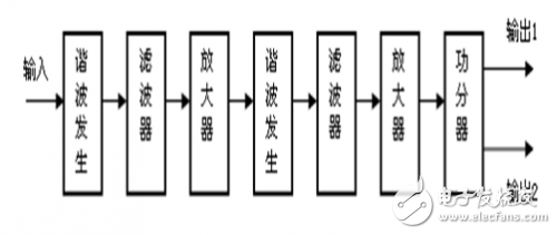
Figure 1 frequency multiplier block diagram
Due to the multiple nonlinear signal processing involved in the transformation process, a rich harmonic component is produced. How to fully and efficiently utilize the required frequency components is the key to the design. The scheme adopts two active frequency multiplications, that is, the frequency multiplication is performed three times, and the other harmonic components are filtered out and then multiplied four times. Since the transistor amplifier has high efficiency and stable and reliable operation, the two-stage harmonic generators are both Implemented with a transistor amplifier. In order to meet the requirements of the total current, the amplifier should not be used too much in the scheme, and the operating power of the amplifier should not be too large. In the actual design, a 3-stage amplifier is selected. In the course of the experiment, we also found that the frequency multiplication efficiency can be improved by adjusting the operating current of the amplifier. The following rules, reducing the current, can reduce the 1dB compression point of the amplifier, which is beneficial to improve the efficiency of the frequency multiplication.
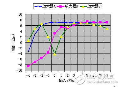
Figure 2 Frequency multiplier input and output power test block diagram
An important indicator of the frequency multiplier is stability over a wide temperature operating range. The operating point of the transistor is susceptible to temperature variations, resulting in large fluctuations in the output power of the multiplied signal. An important factor affecting the operational stability of the multiplier is the change in input signal power because the size of the input signal changes the operating bias voltage of the transistor. The effect of the input signal is different for different amplifiers. Figure 2 shows the input and output power of three different amplifiers. The most important measure to improve the above stability is to add negative feedback. The introduction of negative feedback can not only stabilize the output signal. At the same time, the compression point of the transistor is also reduced, making the output harmonic component easier to stabilize.
Impedance matching needs to be considered in the circuit design. Impedance mismatch will cause signal reflection, resulting in lower frequency doubling efficiency, and the output signal power will not meet the index requirements. At the same time, we must pay attention to the electromagnetic compatibility design. In addition to large-area grounding, each amplifier and each unit's power supply adopts strong filtering measures to prevent crosstalk of signal lines from the power supply and avoid crosstalk and spurs.
Another most important indicator of frequency multipliers is harmonic and clutter suppression, which can usually be achieved by designing a suitable filter. The design of the filter should take into account the out-of-band rejection and loss requirements. Too much loss will affect the frequency multiplication efficiency. The difference in the squareness will affect the harmonic and clutter suppression. This design uses a surface acoustic wave filter with a loss of less than 6 dB and an out-of-band rejection of more than 80 dB. Figure 3 shows the measured results of the amplitude-frequency response of the filter.
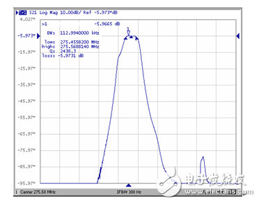
Figure 3 Filter frequency response test results
4 Experimental resultsWhen the input signal is 30MHz and the input power is 3~5dBm, the multiplier output power is greater than 6dBm, the harmonic suppression is greater than 50dB, the power fluctuation is less than 2dB, the operating current is less than 100mA, and the component volume is 70mmX25mmX20mm in the range of -55~85oC. . When the input signal phase noise is ≤ -137dBC/Hz (@10kHz), the output signal phase noise ≤ -114dBC / Hz (@10kHz), compared with the theory deteriorated (137-114) - 20log12 = 1.42dB, mainly due to The noise figure of the first-order transistor is introduced, which is in good agreement with the theory.
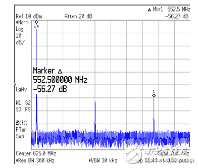
Figure 4 Frequency converter output signal and harmonic suppression measured results
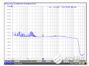
Figure 5 The output signal phase measurement result of the frequency multiplier
5 ConclusionIn this paper, a highly efficient and stable twelve-time frequency multiplier is obtained by using the transistor frequency multiplication method. Since the frequency multiplication implementation is flexible and diverse, it cannot be generalized. The miniaturization, high efficiency, and high frequency band are the future development trends. The design scheme should be reasonably selected according to the specific engineering application environment to obtain a high-performance frequency multiplier.
The cables are for the solar system.
Solar Cable,Pv Wire,Solar Dc Cable,Dc Wire For Solar Panels
NANTONG RONGCHANG IMPORT&EXPORT CO.,LTD , https://www.ergsolarcn.com